
Efficient light-emitting diode containing metal photonic crystal

A technology of metal photonic crystals and light-emitting diodes, applied in semiconductor devices, electrical components, circuits, etc., to achieve the effects of improving directionality, enhancing spontaneous radiation efficiency, and flexible design means

Inactive Publication Date: 2013-07-03
ANHUI NORMAL UNIV
View PDF4 Cites 5 Cited by
  • Summary
  • Abstract
  • Description
  • Claims
  • Application Information

AI Technical Summary

Benefits of technology

This new technology makes it possible for an LED chip that produces white light without any color blinds or filters by combining multiple colors together into one single package instead of requiring separate components like colored glasses. It also increases its luminescence efficacy due to enhanced scattering caused by nanoparticles embedded within the material used to create this special opal-metallic lattice called metamaterial (M) which helps control how much light travels inside them while being blocked from outside viewers. Additionally, there are flexibility ways to customize the M layer's dimensions based on specific needs such as red/greenish blue, yellow, green, cyanosis, etc., allowing for more precise designs overcomes limitations associated with traditional techniques.

Problems solved by technology

This patented technical problem addressed in this patents relates to improving the performance of blue laser diodes for various applications like street lights and indoor displays that require higher brightness levels. Current methods involve increasing the number of layers inside the device's quantum well region, reducing its reflectivity towards ambient environments while also decreasing the amount of emitted light without being wasted. Additionally, current techniques involving modifying the emission process may result in reduced overall optical power transferring from one mode into another mode.

Method used


Image

  • Efficient light-emitting diode containing metal photonic crystal
  • Efficient light-emitting diode containing metal photonic crystal
  • Efficient light-emitting diode containing metal photonic crystal

Examples


Embodiment 1

[0019] In this embodiment, an InGaN light-emitting diode is taken as an example to illustrate the technical solution of the present invention.

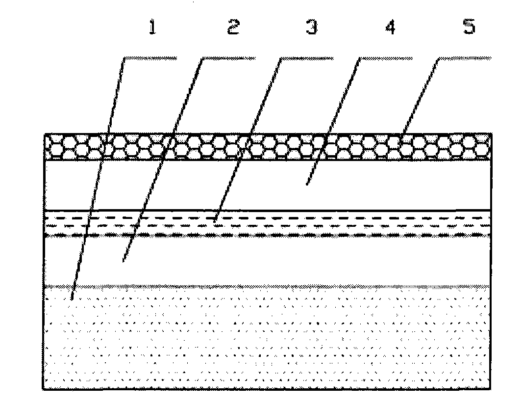
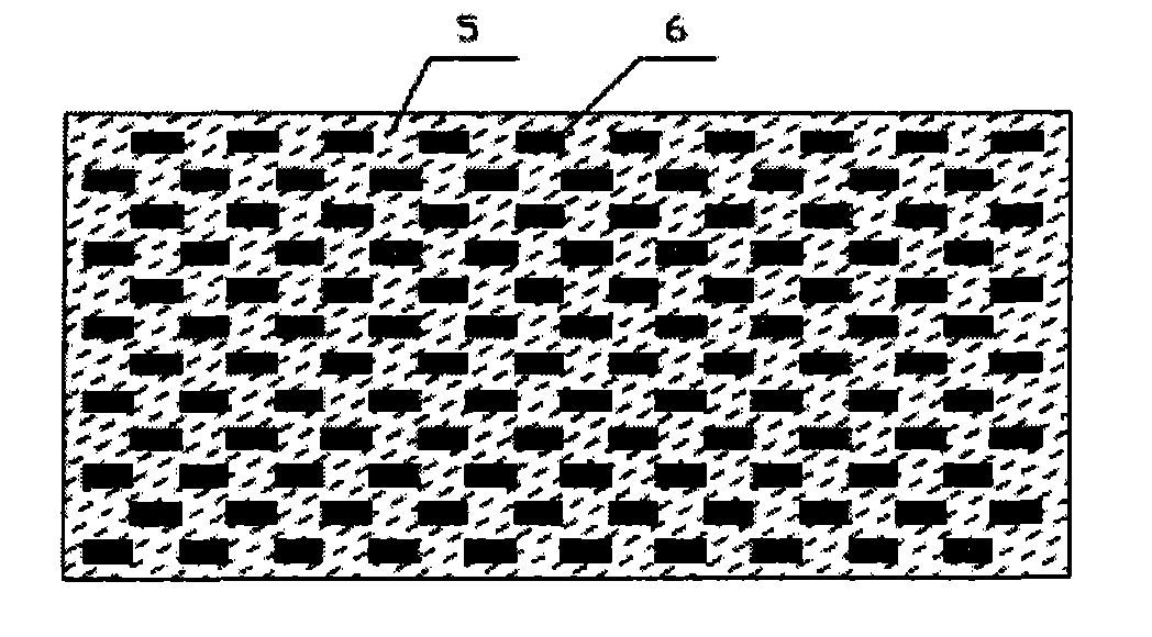
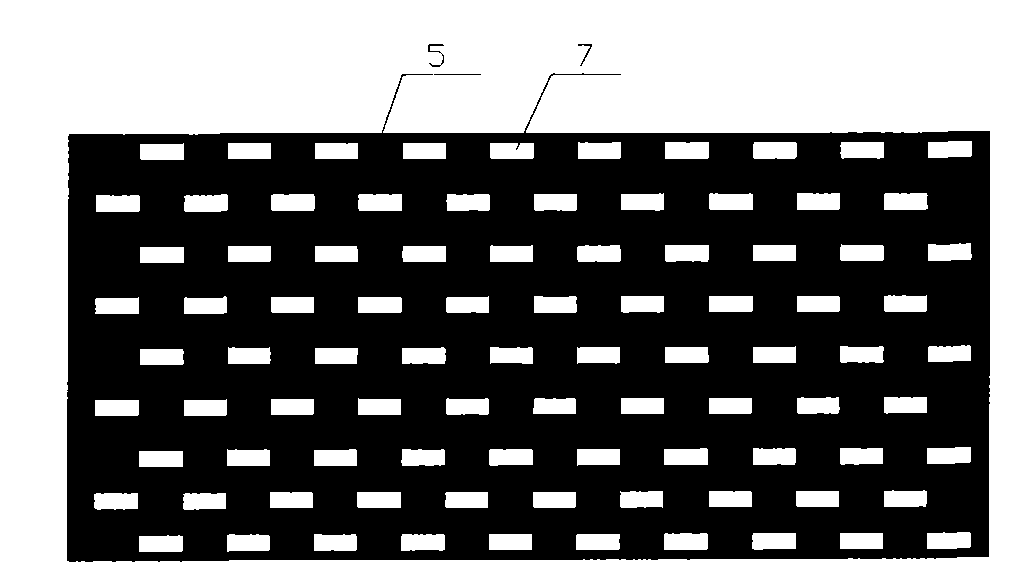
[0020] When the substrate (1) is GaN, the n-type layer (2) is n-GaN, the multiple quantum well (3) is InGaN / GaN, and the p-type layer (4) is p-GaN, the metal photonic crystal (5) is arranged periodically When the dielectric column (6) is formed, it is an InGaN high-efficiency light-emitting diode containing metal photonic crystals.

[0021] The thickness of the metal photonic crystal (5) is 10nm-100nm, and the material can be gold, silver or aluminum. When the light waves emitted by the recombination of carriers and holes in the InGaN / GaN multi-quantum well (3) pass through the p-type layer (4) and radiate outward to the metal photonic crystal (5), surface plasmon waves will be excited. When the thickness of the metal photonic crystal (5) is 10nm-100nm, the periodically arranged dielectric pillars (6) provide reciprocal lattice vecto...


PUM

PropertyMeasurementUnit
Thicknessaaaaaaaaaa

Abstract

The invention discloses an efficient light-emitting diode containing a metal photonic crystal. The efficient light-emitting diode containing the metal photonic crystal is characterized by being composed of a substrate (1), a n-type layer (2), a multi-quantum well (3), a p-type layer (4) and the metal photonic crystal (5), wherein the metal photonic crystal (5) is located above the p-type layer (4). According to the efficient light-emitting diode containing the metal photonic crystal disclosed by the invention, the divergence angle of the outgoing beam of the LED (light-emitting diode) is reduced by virtue of the surface plasmon resonance effect and the energy aggregation effect of the metal photonic crystal, and the photonic band gap light-guiding characteristic of the metal photonic crystal, so that the light-emitting efficiency of the LED can be greatly increased.

Description


Claims


Application Information

Patent Timeline
Owner ANHUI NORMAL UNIV
Learn More