Pixel circuit and driving method thereof, array substrate and display device

A technology for pixel circuits and driving transistors is applied in the fields of pixel circuits and driving methods thereof, display devices, and array substrates, which can solve the problems of unstable circuits, poor image uniformity and poor quality of light emission of organic light-emitting displays, and achieve compensation for non-uniformity, The effect of improved picture uniformity and stable performance

Inactive Publication Date: 2013-07-17
HEFEI BOE OPTOELECTRONICS TECH +1
View PDF10 Cites 18 Cited by
  • Summary
  • Abstract
  • Description
  • Claims
  • Application Information

AI Technical Summary

Problems solved by technology

[0007] The technical problems to be solved by the present invention include, aiming at the problems in the existing pixel unit circuit that the circuit is unstable due to the drift of the threshold voltage of the drive transistor, which leads to the problem of the uniformity of the picture of the organic light-emitting display and the poor quality of the light emission, to provide a device that can Pixel circuit and its driving method, array substrate and display device that effectively compensate for the non-uniformity of the threshold voltage of the driving transistor and improve the picture uniformity of the organic light-emitting display

Method used


Image

  • Pixel circuit and driving method thereof, array substrate and display device
  • Pixel circuit and driving method thereof, array substrate and display device
  • Pixel circuit and driving method thereof, array substrate and display device

Examples


Embodiment 1

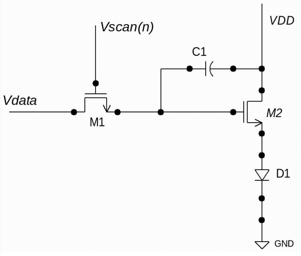
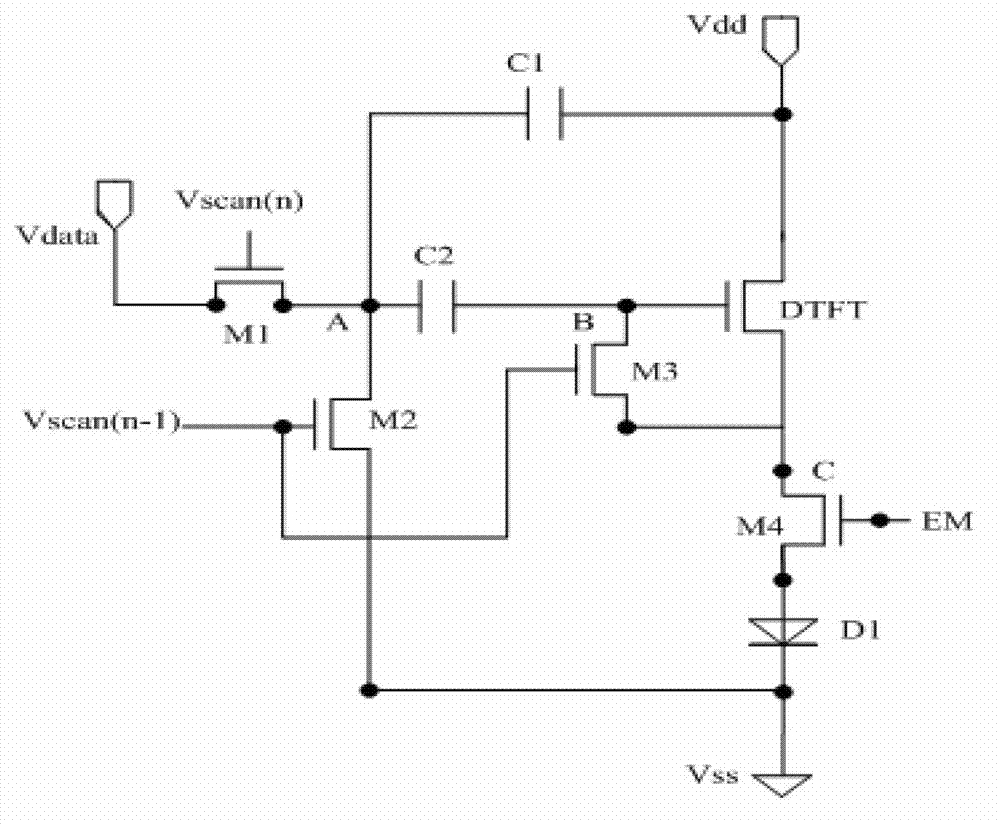
[0033] This embodiment provides a pixel circuit, such as figure 2 As shown, it includes: a driving transistor DTFT, a first switching transistor M1, a storage capacitor C1, a light emitting device, and a threshold compensation circuit; the threshold compensation circuit consists of a second switching transistor M2, a third switching transistor M3, a fourth switching transistor M4 and The coupling capacitor C2 constitutes;

[0034] The gate of M1 of the first switching transistor is connected to the first scan signal Vscan(n), the source is connected to the data signal input terminal Vdata, and the drain is connected to the first end of the storage capacitor C1, the first end of the coupling capacitor C2 and the second switch the source of transistor M2;

[0035] The second terminal of the storage capacitor C1 is connected to the power supply voltage Vdd and simultaneously connected to the source of the driving transistor DTFT;

[0036] The gate of the second switching trans...

Embodiment 2

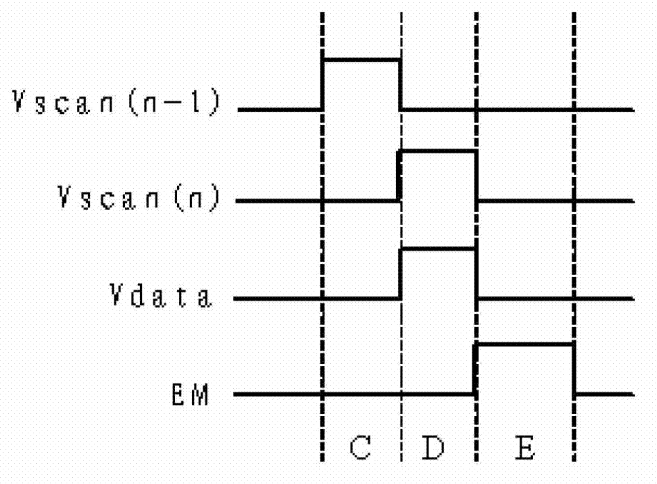
[0056] This embodiment provides a driving method for the above-mentioned pixel circuit, including the following steps:

[0057] Pre-charging stage: the second scan signal Vscan(n-1) and the power supply voltage Vdd are selected, the second switch transistor M2 and the third switch transistor M3 are turned on, and the charge stored in C2 in the coupling capacitor is released , until the voltage at the second end of the coupling capacitor C2 is the threshold voltage of the drive transistor DTFT;

[0058] Compensation stage: the first scan signal Vscan(n) is selected, the first switching transistor M1 is turned on, the second scan signal Vscan(n-1) is turned off, and the data signal Vdata is input to the coupling capacitor C2 The first terminal, the voltage of the second terminal of the coupling capacitor C2 rises and turns on the driving thin film transistor DTFT;

[0059] Light-emitting stage: the first control signal EM is selected, the fourth switching transistor M4 is turne...

Embodiment 3

[0062] This embodiment provides an array substrate, including a plurality of data lines and a plurality of scan lines, the data lines and the scan lines are arranged crosswise, and the pixel circuits in Embodiment 1 are arranged at the intersections.

[0063] This embodiment has the threshold compensation circuit in the pixel circuit in Embodiment 1, which can effectively compensate the non-uniformity of the threshold voltage of the driving transistor DTFT, so that the performance of the array substrate in this embodiment is more stable.


PUM


Abstract

The invention provides a pixel circuit and a driving method thereof, an array substrate and a display device and belongs to the technical field of organic light-emitting display. The pixel circuit comprises a driving transistor, a first switch transistor, a storage capacitor and a light-emitting device and further comprises a threshold compensating circuit. The threshold compensating circuit is formed by a second switch transistor, a third switch transistor, a fourth switch transistor and a coupling capacitor. The threshold compensating circuit can effectively compensate for non-uniformity of threshold voltage of the driving transistor. The driving method comprises a precharge stage, a compensation stage and a light-emitting stage. The array substrate comprises a pixel unit circuit and is stable in performance. The display device comprises the array substrate, and picture uniformity is greatly improved.

Description

technical field [0001] The invention belongs to the technical field of organic light-emitting display, and in particular relates to a pixel circuit and a driving method thereof, an array substrate, and a display device. Background technique [0002] Compared with Thin Film Transisitor Liquid Crystal Display (TFT-LCD), the current mainstream display technology, Organic Light Emitting Diode (OLED) has wide viewing angle, high brightness, high contrast, low energy consumption, and thinner volume Such advantages are the focus of current flat panel display technology. [0003] There are two driving methods of organic light-emitting displays: passive matrix (PM, Passive Matrix) and active matrix (AM, Active Matrix). Compared with the passive matrix drive, the active matrix drive has the advantages of large display information, low power consumption, long device life, and high screen contrast. An equivalent circuit of a pixel unit driving circuit of an active matrix organic light...

Claims


Application Information

Patent Timeline
IPC IPC(8): G09G3/32G09G3/20
CPCG09G3/20G09G3/32G09F9/30G09G3/3233G09G2300/0852G09G2300/0861
Inventor 曾勉尹傛俊涂志中金在光
Owner HEFEI BOE OPTOELECTRONICS TECH
Why Eureka
Try Eureka