Thin film transistor, method of manufacturing thin film transistor, display and electronic device

一种薄膜晶体管、显示器的技术,应用在晶体管、半导体/固态器件制造、电固体器件等方向,能够解决电浅杂质能级氧化物半导体电阻降低等问题,达到抑制晶格缺陷、防止劣化的效果

Active Publication Date: 2017-05-24
JAPAN DISPLAY DESIGN & DEV CONTRACT CO LTD
View PDF7 Cites 0 Cited by
  • Summary
  • Abstract
  • Description
  • Claims
  • Application Information

AI Technical Summary

Problems solved by technology

Lattice defects lead to formation of electrically shallow impurity levels and reduction in resistance of oxide semiconductors

Method used


Image

  • Thin film transistor, method of manufacturing thin film transistor, display and electronic device
  • Thin film transistor, method of manufacturing thin film transistor, display and electronic device
  • Thin film transistor, method of manufacturing thin film transistor, display and electronic device

Examples


no. 1 example

[0068] [structure]

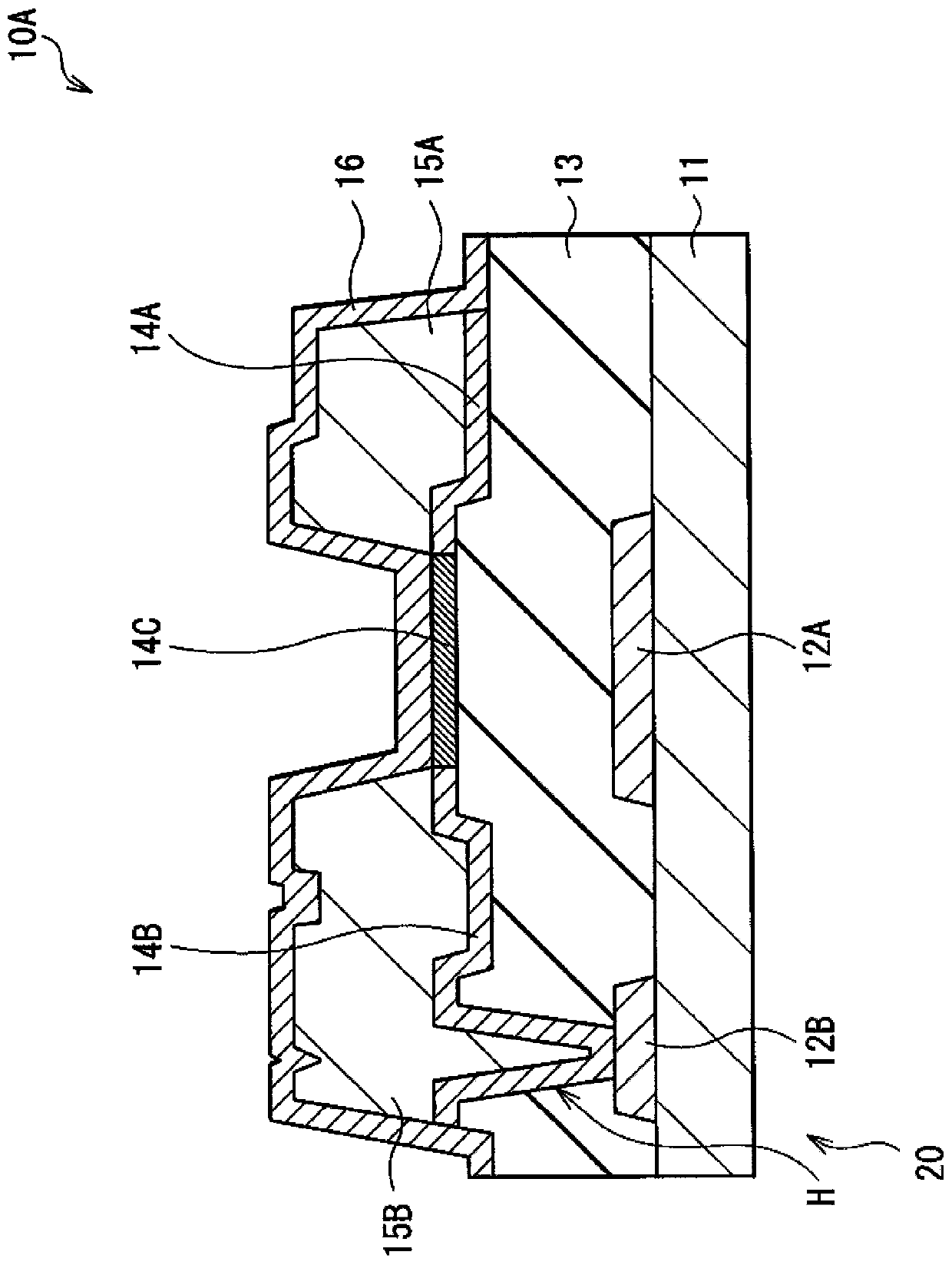
[0069] figure 1 A cross-sectional structure of the thin film transistor (thin film transistor 10A) according to the first embodiment of the present disclosure is shown. The thin film transistor 10A can be used as a driving device in, for example, an active matrix organic EL display (described later) and a liquid crystal display. In the thin film transistor 10A, the oxide semiconductor layer 14C is provided on one surface side of the gate electrode 12A, the gate insulating film 13 is provided between the gate electrode 12A and the oxide semiconductor layer 14C, and the paired source / drain The pole electrodes 15A and 15B are provided to be electrically connected to the oxide semiconductor layer 14C.

[0070] Here, the thin film transistor 10A has a so-called bottom gate structure (reversed overlap structure) and has a gate electrode 12A in a selected region on a substrate 11 formed of, for example, glass. Gate insulating film 13 is formed on the entire su...

no. 2 example

[0107] Figure 12 A cross-sectional configuration of a thin film transistor (thin film transistor 10B) according to the second embodiment of the present disclosure is shown. The thin film transistor 10B has a bottom gate structure like the thin film transistor 10A of the first embodiment described above, and an oxide semiconductor layer 17C is formed on the gate insulating film 13 in a region not facing the source / drain electrodes 15A and 15B. In addition, in regions adjacent to the oxide semiconductor layer 17C and facing the source / drain electrodes 15A and 15B, respectively, low-resistance oxide layers 17A and 17B are formed.

[0108] Each of the oxide semiconductor layer 17C and the low-resistance oxide layers 17A and 17B is formed of an oxide containing an element (for example, indium) similar to that in the oxide semiconductor layer 14C of the first embodiment described above. In addition, each of the low-resistance oxide layers 17A and 17B has a lower resistivity than t...

no. 3 example (

[0123] [Third Embodiment (Thin Film Transistor)]

[0124] Figure 18 A schematic structure (cross-sectional structure) of a thin film transistor (thin film transistor 1020 ) according to the third embodiment is shown. Figure 18 The illustrated thin film transistor 1020 includes a gate electrode 1012, an insulating layer 1013, a channel-formed semiconductor layer 1014, and an electrode layer 1016 formed on an insulating substrate 1011 constructed of a glass substrate or the like. In addition, the insulating layer 1018 is formed to cover the entire thin film transistor 1020 .

[0125] The gate electrode 1012 is formed of metal or alloy such as Mo and Al, and is formed in a predetermined pattern. The insulating layer 1013 will become a gate insulating layer of the thin film transistor 1020 and is formed to cover the gate electrode 1012 . For example, silicon oxide (SiOx) is used as a material of the insulating layer 1013 . The semiconductor layer 1014 is formed of an oxide s...


PUM


Abstract

A thin film transistor includes: a gate electrode, a source electrode, and a drain electrode; an oxide semiconductor layer provided on one side of the gate electrode with an insulating film in between, the oxide semiconductor layer being provided in a region not facing the source electrode and the drain electrode and being electrically connected to the source electrode and the drain electrode; and a low resistance oxide layer provided in a region facing the source electrode and in a region facing the drain electrode, the regions being adjacent to the oxide semiconductor layer, and the low resistance oxide layer having an electric resistivity lower than an electric resistivity of the oxide semiconductor layer.

Description

technical field [0001] The present disclosure relates to thin film transistors (TFTs), methods of manufacturing the same, displays and electronic devices. Background technique [0002] It has been known that oxides (oxide semiconductors) of zinc (Zn), indium (In), gallium (Ga), tin (Sn) or mixtures thereof have excellent semiconductor properties. For example, a thin film transistor using an oxide semiconductor has ten times or more electron mobility than a thin film transistor using amorphous silicon, and a thin film transistor using an oxide semiconductor has favorable off characteristics. Therefore, thin film transistors using oxide semiconductors are expected to be applied to large-screen, high-definition, and high-frame-rate liquid crystal displays or drive devices for organic electroluminescence (EL) displays (see Japanese Patent Application Laid-Open No. 2010-016163). [0003] However, the heat resistance of an oxide semiconductor is insufficient. Therefore, desorpti...

Claims


Application Information

Patent Timeline
Patent Type & Authority Patents(China)
IPC IPC(8): H01L29/786H01L29/06H01L21/336
CPCH01L29/78693H01L27/15H01L29/66742H01L29/66969H01L29/78606H01L29/78618
Inventor 岛山努藤井宣年藤森隆成
Owner JAPAN DISPLAY DESIGN & DEV CONTRACT CO LTD
Why Eureka
Try Eureka