Butted SOI junction isolation structures and devices and method of fabrication
A junction isolation and adjacency technology, applied in semiconductor/solid-state device manufacturing, semiconductor devices, electrical solid-state devices, etc., can solve problems such as short channels and leakage
- Summary
- Abstract
- Description
- Claims
- Application Information
AI Technical Summary
Problems solved by technology
Method used
Image

Examples
Embodiment Construction
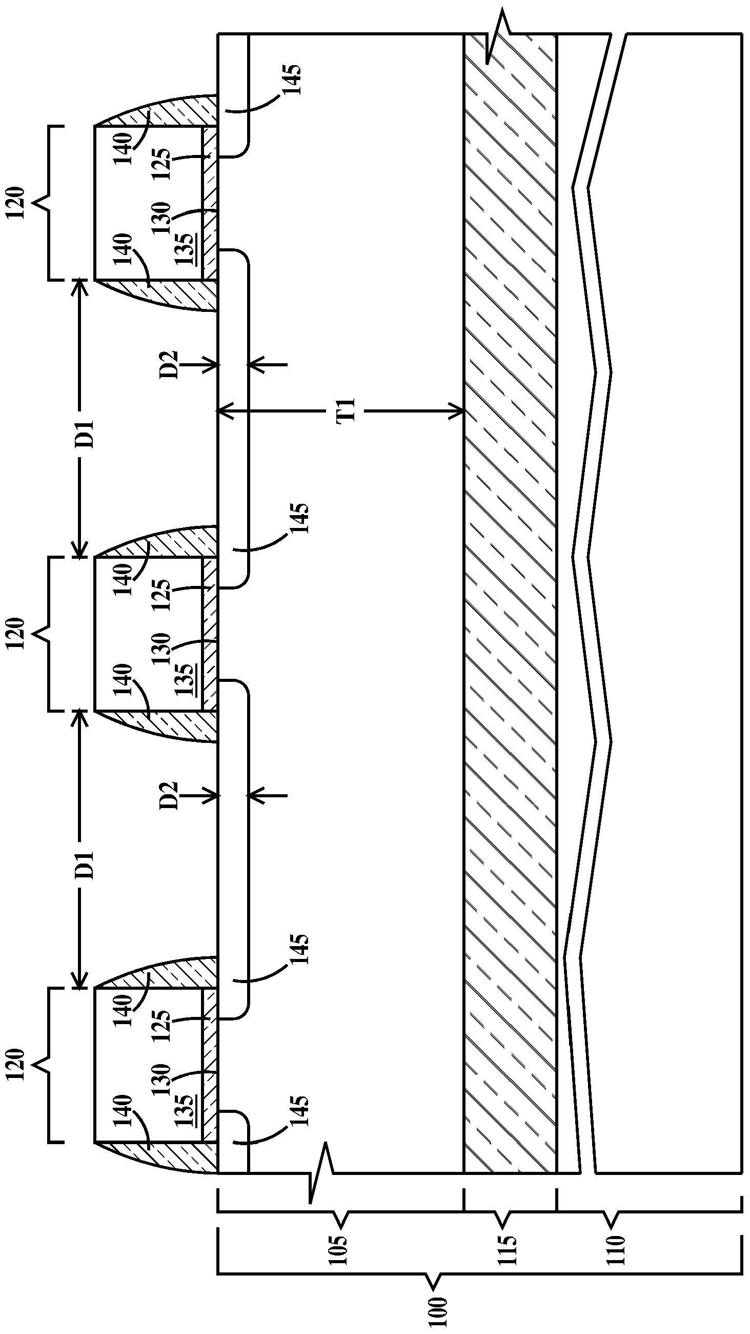
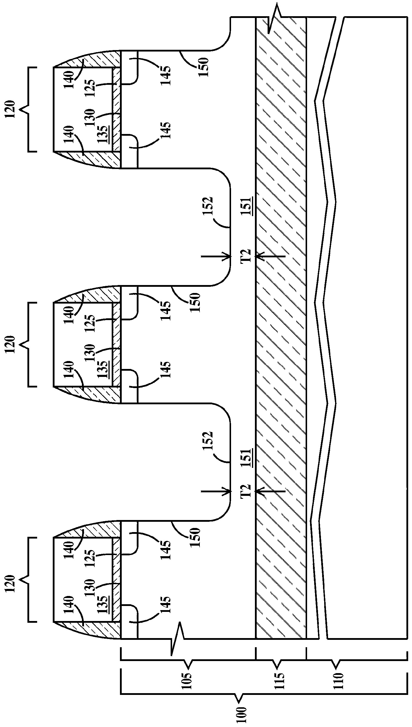
[0015] The term "doping concentration" is defined as the net doping concentration, and the net doping concentration is defined as |N A -N D |, where N A is the concentration of acceptor atoms and N D is the concentration of donor atoms. Acceptor atoms dope silicon (Si) to P-type. Boron (B) is an example of a P-type dopant. Donor atoms dope the silicon N-type. Phosphorus (P) and arsenic (As) are examples of N-type dopants. The term "intrinsic" in relation to silicon is defined as silicon without (P or N) type dopant species, i.e. N A =0 and N D =0. Thus, the intrinsic silicon layer should be compatible with zero net doping ie |N A -N D |=0, where N A ≠0 and N D ≠0 silicon layers are distinguished. The term "net dopant type" is defined as a dopant type of higher concentration of dopant species. When N A >N D , the silicon is net-doped P-type, where N A D ≠0 or N D =0. When N D >N A , the silicon is net-doped N-type, where N D A ≠0 or N A =0. The term "epi...
PUM
 Abstract
Description
Claims
Application Information