A method for preparing trench semiconductor discrete devices

A discrete device and semiconductor technology, applied in semiconductor/solid-state device manufacturing, electrical components, circuits, etc., can solve problems such as poor terminal structure, poor device breakdown voltage and reliability, and difficult to generate

Inactive Publication Date: 2016-06-22
立新半导体有限公司
View PDF6 Cites 0 Cited by
  • Summary
  • Abstract
  • Description
  • Claims
  • Application Information

AI Technical Summary

Problems solved by technology

[0005] In the existing trench power MOSFET design and manufacturing field, the base region and the source region of the MOSFET are introduced by the steps of base region mask and source region mask respectively. In order to reduce the manufacturing cost, some previous proposals, For example, the published US patent documents US20110233667, US20090085074, US20110233666, US077996427, etc., try to omit the manufacturing method of the base region or source region mask step, the steps are relatively complicated and difficult to generate, and the terminal (termination) structure of the manufactured semiconductor device Not good, so that the breakdown voltage and reliability of the device are relatively poor

Method used


Image

  • A method for preparing trench semiconductor discrete devices
  • A method for preparing trench semiconductor discrete devices
  • A method for preparing trench semiconductor discrete devices

Examples


Embodiment 1

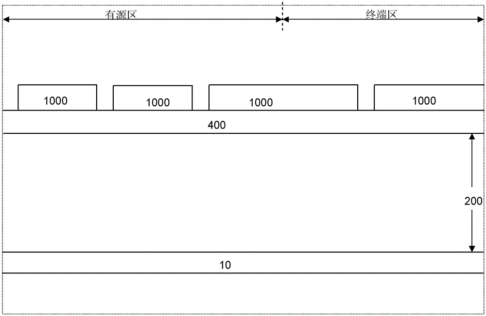
[0082] Such as figure 1 As shown, the epitaxial layer 200 is placed above the substrate 10. First, an oxide layer 400 (with a thickness of 0.3 μm to 1.5 μm oxide hard mask) is formed on the epitaxial layer by deposition or thermal growth, and then on the oxide layer. A photoresist coating 1000 is deposited and then patterned through a trench mask to expose portions of the oxide layer.

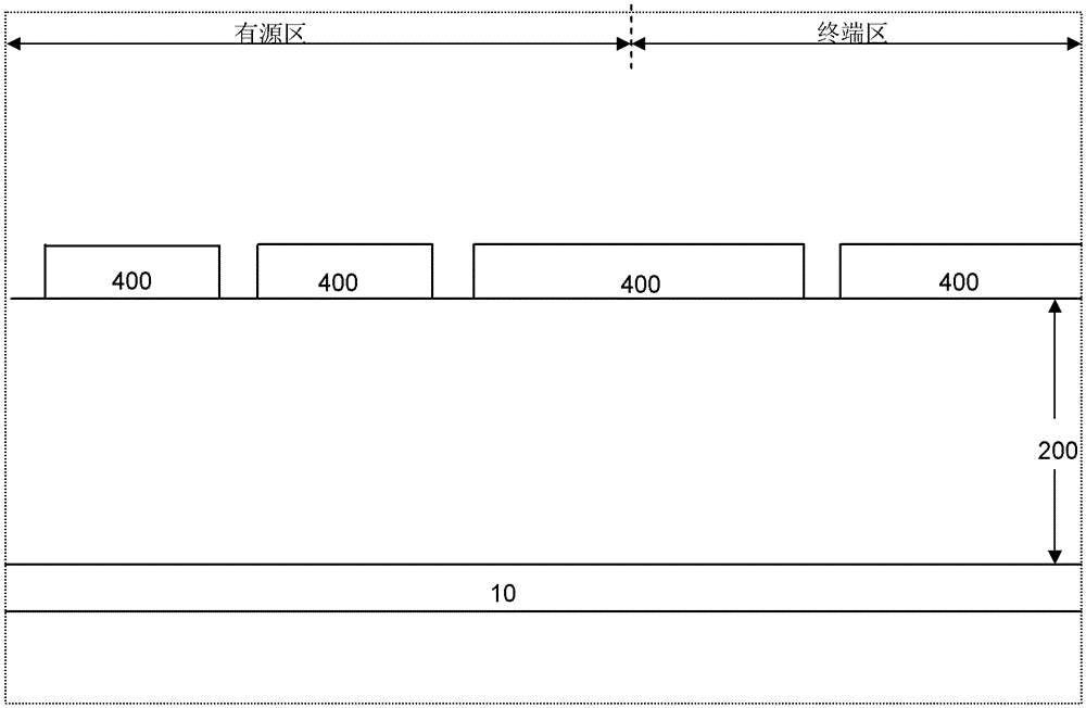
[0083] Such as figure 2 As shown, after dry etching the oxide layer exposed by patterning the trench mask, the epitaxial layer is exposed, and then the photolithographic coating is removed.

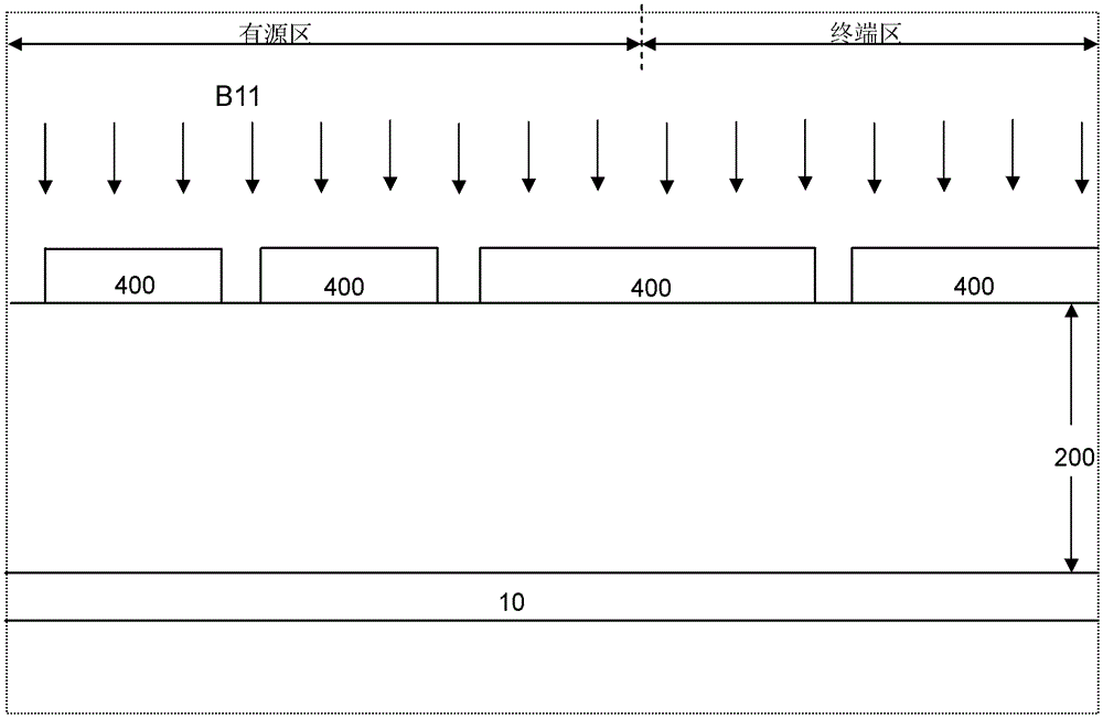
[0084] Such as image 3 As shown, implant P-type dopants on the surface of the silicon wafer (the dose is 2e12 / cm 3 to 2e14 / cm 3 ), the part covered by the original oxide layer 400 has not been implanted, and the part not covered by the original oxide layer will be injected into the surface of the epitaxial layer to form a P-type region. The P-type dopant can be B11 (boron boron ).

[0085] Such as ...

Embodiment 2

[0100] The technical scheme of the present embodiment is roughly the same as that of embodiment 1, and its difference only lies in:

[0101] In the above example 1 Figure 5 Before etching the trench, first deposit a layer of oxide layer and seal the opening width of the trench mask in the oxide layer ranging from 0.2 μm to 0.6 μm. The width of the sealed opening can be 0.2 μm or 0.3 μm or 0.4 μm or 0.5 μm or 0.6 μm, depending on the preparation method, the advantage of this step is that some trench mask openings are implanted with P-type dopants (P-type 1 region) but not The trench is opened, the terminal structure of the device is better, so the breakdown voltage of the device is higher and more stable, and then the oxide layer is dry-etched to remove the oxide layer on the opening and expose the epitaxial layer on the opening; After etching the trench, only those openings that are not sealed by the precipitated oxide layer are opened. The trench (1.0 μm to 7.0 μm in depth ...

Embodiment 3

[0103] The technical scheme of the present embodiment is roughly the same as that of embodiment 1, and its difference only lies in:

[0104] In the above example 1 Figure 15 Before etching the contact hole trench, first deposit a layer of (LPCVD) oxide layer, and then perform dry etching on the oxide layer to remove the oxide layer in the opening of the contact hole trench, exposing the epitaxial layer in the opening; etched contact hole trenches. Other steps are basically the same as in Embodiment 1, and the cross-section of the device is as follows Figure 19 shown.


PUM


Abstract

The invention discloses a method of preparing a groove discrete semiconductor device. The method comprises the following steps: first, injecting P type dopant into an epitaxial layer of a substrate to form a P type area I by using a groove mask, and carrying out etching on the external layer to form a plurality of grid electrode grooves; then depositing interlamination media on the surface of the external layer, carrying out etching on the interlamination media by using a contact hole mask to form openings in the interlamination media, and injecting the P type dopant and N type dopant to the openings to form a P type area II and an N type source region respectively, wherein the P type area I and the P type area II are combined into a P type base region; then carrying out etching on the surface of the external layer to form contact hole grooves, and carrying out metal plugging filling on the contact hole grooves; and finally, depositing a metal layer on the surface of a device, carrying out metal etching by using metal mask to form a metal cushion layer and connection wires. By adopting the method of preparing the groove discrete semiconductor device, preparation procedures of base region masking and source region masking are eliminated, and the preparation cost of the device is made to be greatly reduced.

Description

technical field [0001] The invention relates to the technical field of semiconductor power discrete devices, in particular to a method for preparing a trench semiconductor power discrete device. Background technique [0002] At present, power MOSFET (MetalOxideSemiconductorFieldEffectTransistor, Metal Oxide Semiconductor Field Effect Transistor) has been widely used in various electronic and communication products, computers, consumer appliances, automobiles, etc. At the same time, it also has various applications in industry. [0003] Power semiconductor devices represented by power MOSFETs can effectively control high-frequency large currents due to their low on-resistance and high-speed switching. At the same time, power MOSFETs are being widely used as small power conversion components such as power amplifiers, power converters, low noise amplifiers, and some personal computer power supply switches and power circuits, which are characterized by low power consumption and ...

Claims


Application Information

Patent Timeline
Patent Type & Authority Patents(China)
IPC IPC(8): H01L21/336
Inventor 苏冠创
Owner 立新半导体有限公司
Why Eureka
Try Eureka