Method for testing free carrier absorption loss and battery sample

A carrier absorption and free technology, which is applied in the field of solar cells, can solve the problems of increasing the cost of testing methods, increasing the investment of testing costs, and complicated testing methods, so as to save investment in equipment costs, fast testing, and wide testing range. Effect

Pending Publication Date: 2022-06-28
TAIZHOU ZHONGLAI PHOTOELECTRIC TECH CO LTD
View PDF0 Cites 0 Cited by
  • Summary
  • Abstract
  • Description
  • Claims
  • Application Information

AI Technical Summary

Problems solved by technology

[0005] However, this conventional method is extremely complex, time-consuming, and expensive to test: for example, steps 1) and 2) require the preparation of battery samples with different structures to obtain optical constants (i.e., n values ​​and k values) and measured data respectively (i.e. the data of reflectance, transmittance and spectral response), which makes the test method complicated, cumbersome, and time-consuming; and step 1) needs to use special equipment—full spectrum ellipsometer to obtain n value and k value , which increases the input of test cost; the extraction of n value and k value, and the collection of multiple measured data of reflectivity, transmittance and spectral response also make the test method more complicated and time-consuming; Moreover, as the input of the simulation software of Sentaurus, and the simulation and fitting process of step 3) usually need to adopt large-scale server to carry out calculation, these further increase the cost input of this test method, and make the test method become more loaded down with trivial details, and takes longer

Method used


Image

  • Method for testing free carrier absorption loss and battery sample
  • Method for testing free carrier absorption loss and battery sample
  • Method for testing free carrier absorption loss and battery sample

Examples


Embodiment 1

[0085] A method for testing free carrier absorption loss in this embodiment includes the following steps:

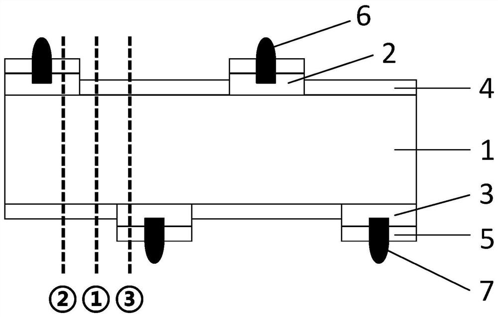
[0086] Step 1. Prepare battery samples of specific structure (see figure 1 ):

[0087] Step 11. Select silicon wafer 1 with N-type conductivity, resistivity of 7Ω·cm, and thickness of 160 μm, perform damage removal treatment on silicon wafer 1, texture, and then perform single-sided polishing on the rear surface of silicon wafer 1 , to obtain a silicon wafer 1 with a textured front surface and a polished rear surface.

[0088] Step 12 , respectively forming a front heavily doped layer and a rear heavily doped layer with opposite conductivity types on the front surface and the rear surface of the silicon wafer 1 . In actual operation, boron ion implantation is performed on the front surface of the silicon wafer 1 by means of ion implantation, and phosphorus ion implantation is performed on the rear surface of the silicon wafer 1, followed by annealing treatment to activ...

Embodiment 2

[0105] For a method for testing free carrier absorption loss in this embodiment, refer to Embodiment 1 for specific steps, and the difference from Embodiment 1 is as follows:

[0106] In step 11, the resistivity of the selected silicon wafer 1 is 5Ω·cm.

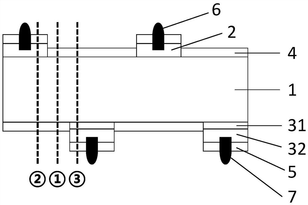
[0107] In step 12, see image 3 , the preparation process of the front heavily doped layer on the front surface of the silicon wafer 1 is the same as that in Example 1, and the rear surface of the silicon wafer 1 is changed to deposit an ultra-thin tunnel oxide layer 31 and an in-situ phosphorus-doped polysilicon layer ( Namely, the heavily doped polysilicon layer 32), therefore, after annealing, a passivation contact structure composed of the tunnel oxide layer 31 and the phosphorus-doped polysilicon layer is formed on the rear surface of the silicon wafer 1 as the rear heavily doped layer.

[0108] The square resistance of the front heavily doped layer (corresponding to the first heavily doped layer 2 ) in this embodiment ...

Embodiment 3

[0115] For a method for testing free carrier absorption loss in this embodiment, refer to Embodiment 1 for specific steps, and the difference from Embodiment 1 is as follows:

[0116] In step 11, the resistivity of the selected silicon wafer 1 is 5Ω·cm, and the conductivity type is P-type.

[0117] In step 12, see Figure 5 , the front surface of the silicon wafer 1 is implanted with phosphorus ions, so after annealing, a phosphorus-doped emitter is formed on the front surface of the silicon wafer 1, that is, the front heavily doped layer; and the rear surface of the silicon wafer 1 is not doped , so the rear heavily doped layer of Example 1 is omitted. The square resistance of the front heavily doped layer (corresponding to the first heavily doped layer 2) is 90-120Ω / sq, the junction depth is 0.4-0.6μm, and the peak concentration is 6.0-8.0E+19cm -3 .

[0118] In step 13, the locally disposed second heavily doped layer 3 and its preparation process are omitted, so the batt...


PUM

PropertyMeasurementUnit
depthaaaaaaaaaa
thicknessaaaaaaaaaa
thicknessaaaaaaaaaa

Abstract

The invention belongs to the technical field of solar cells, and provides a method for testing free carrier absorption loss and a cell sample, and the method comprises the steps: preparing a cell sample with a specific structure, the battery sample comprises a first region, a second region and a third region; the first region is provided with a first heavily-doped layer on the front surface and then a second heavily-doped layer on the rear surface; the third region is provided with a second heavily-doped layer on the front surface and then a second heavily-doped layer on the rear surface; testing the external quantum efficiency of the first area, the second area and the third area in the near-infrared band; obtaining integral current density values of the first region, the second region and the third region according to the external quantum efficiency and the AM1.5 G spectrum of the first region, the second region and the third region; and obtaining the free carrier absorption loss according to the integral current density values of the first region, the second region and the third region. The method is simpler in test, short in time consumption and low in cost, and can quickly and accurately realize quantitative detection of free carrier absorption loss.

Description

technical field [0001] The invention relates to the technical field of solar cells, in particular to a method for testing the absorption loss of free carriers and a battery sample. Background technique [0002] Crystalline silicon solar cells are a common type of solar cells. Optical losses in crystalline silicon solar cells mainly include: metal grid line shielding loss, reflection loss, escape loss, transmission loss, recombination loss, and free carrier absorption loss. Among them, free carrier absorption refers to photons close to the semiconductor band gap energy (interband absorption is very weak), which is absorbed by free electrons or holes in the semiconductor material, resulting in intra-band transitions, and the energy of photons is finally consumed in the form of heat energy Dissipated and does not contribute to the photocurrent, which belongs to parasitic absorption. In crystalline silicon solar cells, the absorption of free carriers is particularly significan...

Claims


Application Information

Patent Timeline
Patent Type & Authority Applications(China)
IPC IPC(8): G01R31/385G01R31/26G01N21/359H01L31/06H01L31/18
CPCG01R31/385G01R31/2601G01N21/359H01L31/1804H01L31/06Y02E10/50
Inventor 陈嘉王倩包杰季根华沈承焕杜哲仁
Owner TAIZHOU ZHONGLAI PHOTOELECTRIC TECH CO LTD
Why Eureka
Try Eureka