Touch display panel

A touch display panel and touch sensing technology, applied in static indicators, optics, instruments, etc. Reduced transmittance and other issues, to achieve the effect of improving light transmittance and thinning the overall thickness

Inactive Publication Date: 2013-08-14
WINTEK CHINA TECH LTD +1
View PDF4 Cites 13 Cited by
  • Summary
  • Abstract
  • Description
  • Claims
  • Application Information

AI Technical Summary

Problems solved by technology

[0003] However, the touch panel and the display panel each have substrates carrying their respective components. After the touch panel and the display panel are laminated, although a touch display panel with touch and display functions is formed, its overall thickness cannot be effectively reduced. , unable to meet consumers' demand for thin, light and small electronic products
In addition, in this prior art, since the display light must pass through the multi-layer substrate, the overall light transmittance of the touch display panel decreases.

Method used


Image

  • Touch display panel
  • Touch display panel
  • Touch display panel

Examples


no. 1 example

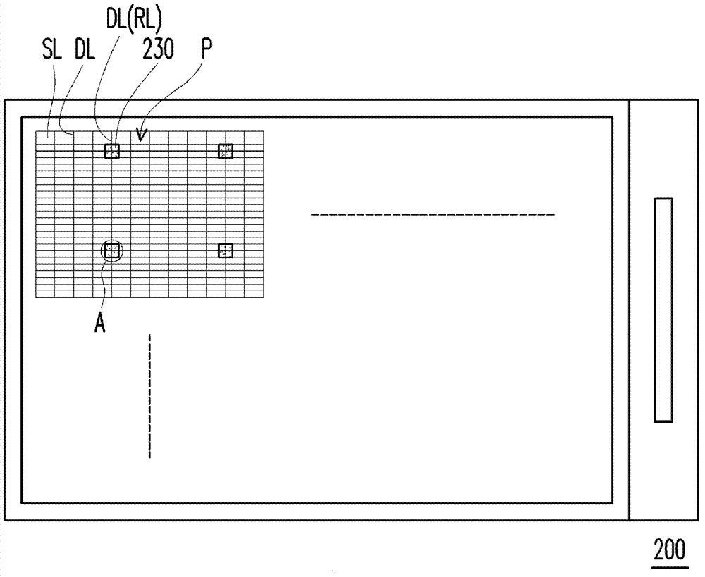
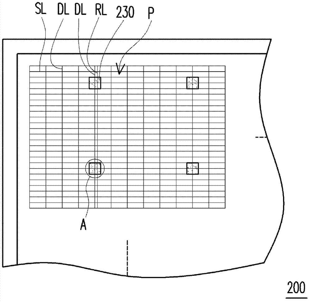
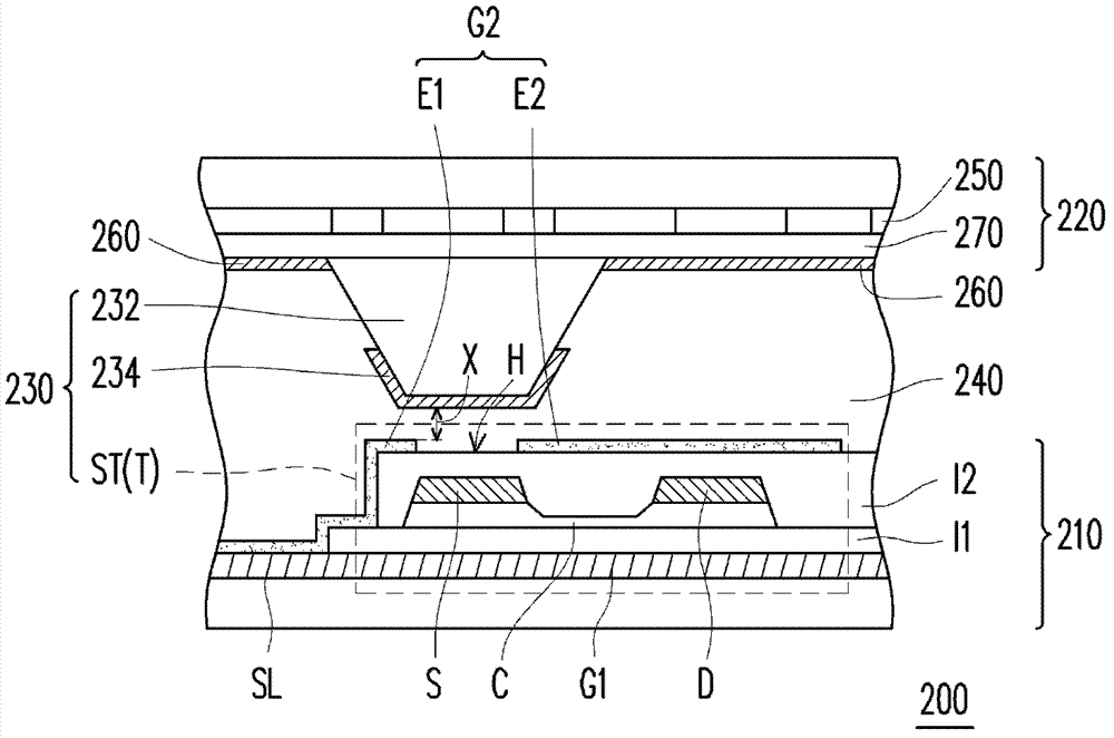
[0050] Figure 1A is a schematic top view of a touch display panel in the first embodiment of the present invention, and Figure 2A for Figure 1A The enlarged cross-sectional schematic diagram at A. Such as Figure 1A and Figure 2A As shown, the touch display panel 200 includes a first substrate 210, a second substrate 220 opposite to the first substrate 210, a plurality of touch sensing structures 230 and a display medium 240 between the two substrates 210 and 220. . The display medium 240 includes liquid crystal molecules or other display mediums.

[0051] In this embodiment, the first substrate 210 is an active device array substrate, on which a plurality of pixel structures P arranged in an array, a plurality of scan lines SL, a plurality of data lines DL and at least one readout line RL are disposed. In more detail, each pixel structure P may include an active element T and a pixel electrode (not shown) electrically connected thereto, wherein each active element T is...

no. 2 example

[0061] Figure 6A for Figure 1A Another schematic cross-sectional view enlarged at A, and Figure 6B for right Figure 6A A schematic cross-sectional view of the touch display panel after pressing. The touch display panel 300 of the second embodiment is similar to the touch display panel 200 of the first embodiment, except that the control of the sensing active element ST in the touch display panel 300 of this embodiment is only controlled by the bottom before the touch. The gate G1 is controlled, and after the touch, it is controlled by both the top gate G2 and the bottom gate G1.

[0062] In this embodiment, the opening H of the top gate G2 partially overlaps the channel C in the projection direction of the first substrate 210, but it is not limited to being centered or sideways, and if necessary, does not affect the aperture ratio of the display unit. It is also possible not to overlap with the channel C of the sensing active device ST, and the bottom gate G1 is under t...


PUM


Abstract

The invention relates to a touch display panel which comprises a first substrate, a second substrate, a plurality of touch sensing structures, and a display medium. The first substrate is provided with a plurality of pixel structures, a plurality of scanning lines, and a plurality of reading lines. Each touch sensing structure comprises a sensing active element, a touch clearance part and a bridge electrode. Each of the sensing active elements located on the first substrate comprises a bottom gate, a channel, a source, a sensing electrode and a top gate. Each top gate is provided with an opening, thereby being electrically divided into a first electrode and a second electrode. The touch clearance parts and the bridge electrodes are located on a second substrate above the opening. When the touch display panel is touched, the bridge electrodes contact with the top gates to electrically connect the first and second electrodes, the channel is controlled by both of the top gates and the bottom gates instead of being controlled by one of the top gates and the bottom gates, and the sensing electrodes generate sensing current.

Description

technical field [0001] The invention relates to an electronic device, in particular to an integrated touch panel and a touch display panel. Background technique [0002] Generally speaking, for the touch display panel, the touch panel is attached to the display panel, so that the touch display panel has the functions of touch sensing and display. The touch panel usually includes a plurality of first sensing series extending along the X-axis direction, and a plurality of second sensing series extending along the Y-axis direction, wherein each first sensing series is connected to each The second sensing series respectively has a plurality of sensing pads connected in series. When a finger touches the touch panel, the capacitance between the sensing pads will be changed, and the change signal will be sent back to the controller to calculate the coordinates of the touch point, so that the display panel can be adjusted according to the user's choice. Change the display screen. ...

Claims


Application Information

Patent Timeline
Patent Type & Authority Applications(China)
IPC IPC(8): G06F3/041G02F1/133G02F1/1362
Inventor 周建良苏振豪
Owner WINTEK CHINA TECH LTD
Why Eureka
Try Eureka