In-mould decoration material
A technology of in-mold decoration and transfer printing materials, which is applied in the direction of decorative art and the process for producing decorative surface effects, etc. It can solve the problems of yield rate and process difficulties, and the inability to make microstructure patterns, etc., to improve color saturation, Increased tactile effect
- Summary
- Abstract
- Description
- Claims
- Application Information
AI Technical Summary
Problems solved by technology
Method used
Image

Examples
no. 1 example
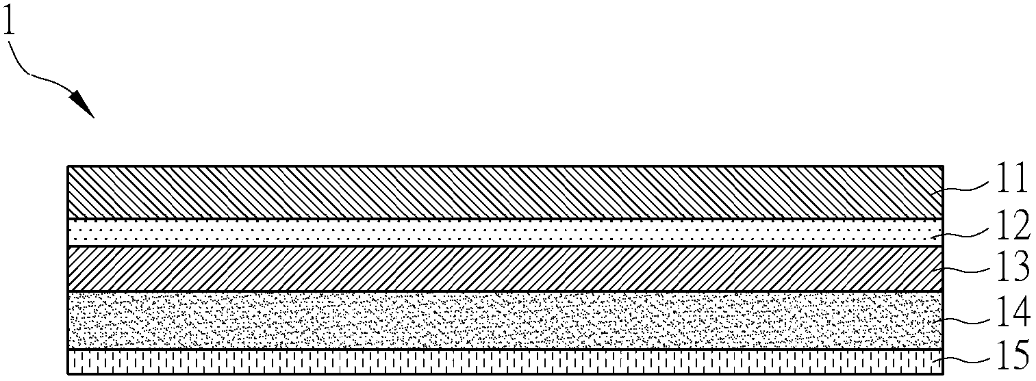
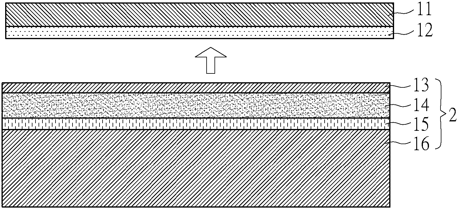
[0075] Please refer to Figure 4 Shown is a schematic diagram of the flexible mold of the first embodiment of the present invention. The flexible mold 3 of this embodiment is used in the three-dimensional structure transfer printing process. The so-called three-dimensional structure transfer printing process includes thermal transfer printing, three-dimensional thermal transfer printing, in-mold injection transfer printing, and water transfer printing. A three-dimensional structure or pattern is produced, and the mold used therein includes but is not limited to a roller or a plate.
[0076] The flexible mold 3 includes a base material 31 and a microstructure pattern layer 32, the microstructure pattern layer 32 is a layer with a microstructure pattern surface, the microstructure pattern layer 32 has a first pattern 321, and the first pattern 321 is located in the microstructure pattern. On the surface of the structural pattern layer 32 , the microstructure pattern layer 32 is...
no. 2 example
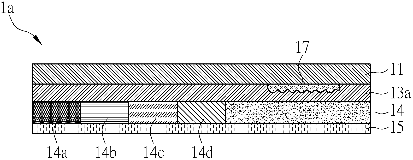
[0089] Please refer to Figure 9A and Figure 9B shown, where Figure 9A is a schematic diagram of the flexible mold of the second embodiment of the present invention, Figure 9B It is a schematic top view of the microstructure pattern layer of the flexible mold of the second embodiment. The flexible mold 3a includes a substrate 31 and a microstructure pattern layer 32a, and the microstructure pattern layer 32a has a first sub-pattern 322 of a hairline pattern and a second sub-pattern 323 of a three-dimensional pattern . Wherein, the material of the substrate 31 can be polyethylene terephthalate (Polyethylene Terephthalate, PET), polycarbonate (polycarbonate, PC), non-extended polypropylene (Casted Polypropylene, CPP), co-extruded oriented polypropylene Propylene (Oriented polypropylene, OPP). And the thickness of the substrate 31 is 10 μm to 250 μm. In this embodiment, the substrate 31 is exemplified by polyethylene terephthalate (PET) with a thickness of 50 μm.
[009...
PUM
| Property | Measurement | Unit |
|---|---|---|
| thickness | aaaaa | aaaaa |
| thickness | aaaaa | aaaaa |
| thickness | aaaaa | aaaaa |
Abstract
Description
Claims
Application Information
 - R&D Engineer
- R&D Manager
- IP Professional
- Industry Leading Data Capabilities
- Powerful AI technology
- Patent DNA Extraction
Browse by: Latest US Patents, China's latest patents, Technical Efficacy Thesaurus, Application Domain, Technology Topic.
© 2024 PatSnap. All rights reserved.Legal|Privacy policy|Modern Slavery Act Transparency Statement|Sitemap