Color film substrate, production method thereof and liquid crystal panel

A manufacturing method and color filter substrate technology, applied in the fields of instruments, nonlinear optics, optics, etc., can solve the problem of low spacer support area ratio, the inability to further increase the aperture ratio of the pixel area, and low transmittance of the pixel aperture ratio, etc. problem, to achieve the effect of low production cost

Active Publication Date: 2013-08-21
BOE TECH GRP CO LTD +1
View PDF4 Cites 26 Cited by
  • Summary
  • Abstract
  • Description
  • Claims
  • Application Information

AI Technical Summary

Problems solved by technology

However, since the thickness of each layer in the array substrate is relatively fixed, the height difference between spacers of different heights made in this way is also relatively fixed, so that the adjustment range of the corresponding liquid crystal filling amount becomes relatively limited.
In addition, since the spacers of different heights need to be made by using this method to utilize the own level difference of the array substrate, the spacers need to be set according to the position of the level difference, so that the places where the spacers are allowed to be placed in the design become very limited. Usually, there are certain requirements for the position of the spacer
like image 3 As shown, the relatively tall spacers (the spacers that are in contact with the steps on the array substrate) and the relatively short spacers (the spacers that are not in contact with the steps on the array substrate) should be set on the black Between two adjacent light-transmitting areas on the matrix, a certain distance should generally be reserved between the spacer and each light-transmitting area to avoid pixel light leakage caused by poor rubbing orientation, which makes the design of the black matrix The position of the spacer needs to be accommodated, so the aperture ratio of the pixel area cannot be further improved. A lower pixel aperture ratio will bring a lower transmittance, and a lower transmittance is not conducive to high PPI ( Pixel Per Inch, pixel density, the number of pixels per inch, used to characterize the display fineness of display devices)
On the other hand, the size (diameter) of spacers formed in this way is generally smaller than that of ordinary spacers (that is, their diameters are smaller than figure 1 and figure 2 The diameter of the spacer shown in ), the smaller size of the spacer will bring a lower proportion of the supporting area of ​​the spacer, which is not conducive to the performance of the pressing strength of the display panel, and is not conducive to the increasingly wide range of touch screen terminal applications
In addition, due to the pursuit of higher display quality, in the current high-end display panel products, the Overcoat (flat layer) material is also used to planarize the array substrate to form a flat layer. The result is , the surface of the array substrate is basically flat, so there is no image 3 The level difference layer 9 that can be used in , if the spacers with the same absolute height are still used, it is impossible to achieve multiple heights of spacers in high-end display panels

Method used


Image

  • Color film substrate, production method thereof and liquid crystal panel
  • Color film substrate, production method thereof and liquid crystal panel
  • Color film substrate, production method thereof and liquid crystal panel

Examples


Embodiment 1

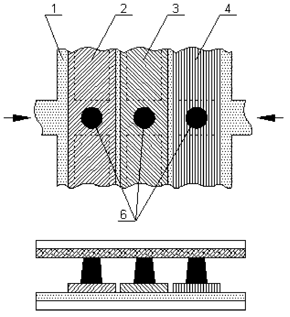
[0093] This embodiment provides a method for manufacturing a color filter substrate, including the following steps:

[0094] Step 1: setting a bottom pad at the designed position of the spacer on the first substrate;

[0095] Step 2: arranging spacers on the bottom pad and other designed positions of spacers without a bottom pad on the first substrate to form spacers with different heights; or, the bottom pad There are two or more different heights, and spacers are respectively arranged on the bottom pads of different heights to form spacers with different heights.

[0096] The color filter substrate includes a first substrate and a plurality of functional layers arranged on the first substrate.

[0097] Wherein, in step 1, the bottom pad can be directly or indirectly arranged on the first substrate. The so-called indirect installation means that the bottom pad is arranged on each functional layer on the first substrate without direct contact with the first substrate, such as...

Embodiment 2

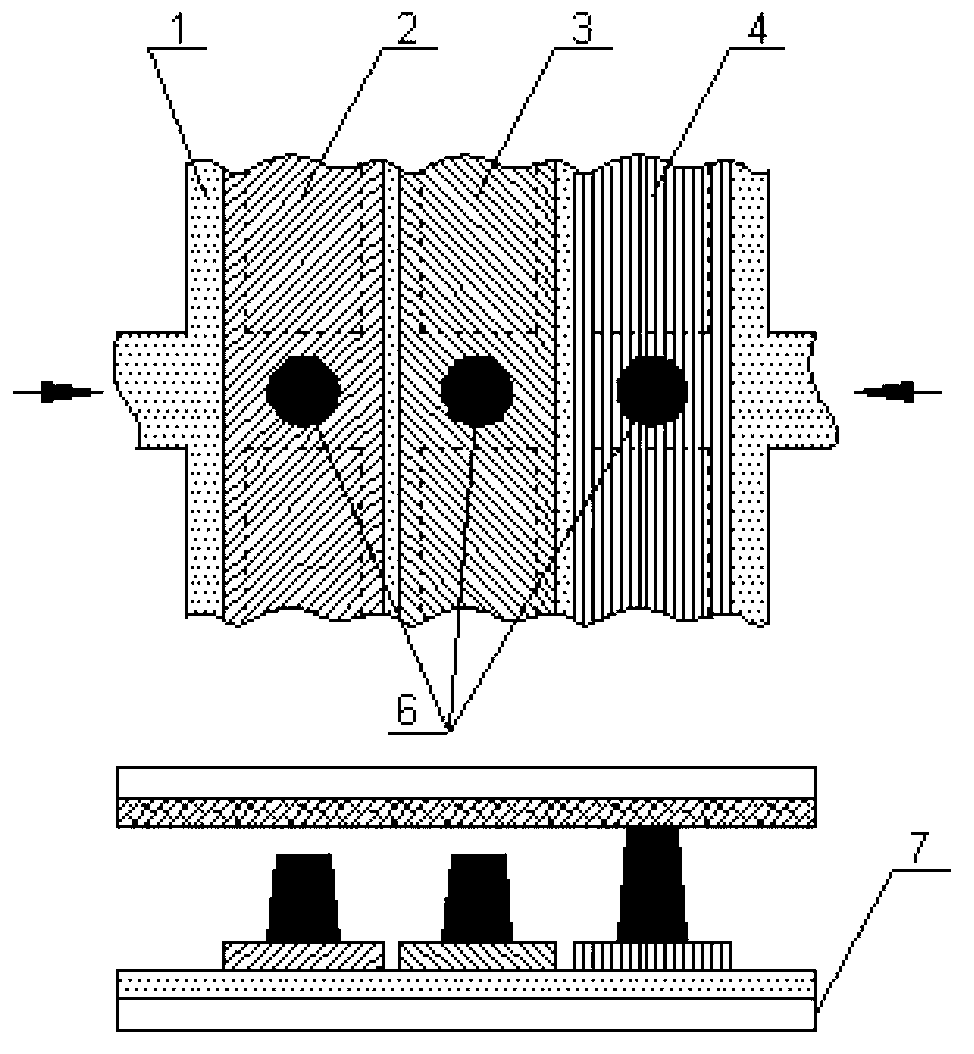
[0099] This embodiment provides a method for manufacturing a color filter substrate, including the following steps:

[0100] Step 1: setting the bottom pad 8 at the designed position of the spacer on the first substrate;

[0101] Step 2: setting spacers of the same height on the bottom pad and other designed positions of the spacers without bottom pads on the first substrate 7 to form spacers with different heights; or, The bottom pads have two or more different heights, and spacers of the same height are respectively arranged on the bottom pads of different heights to form spacers with different heights.

[0102] Since the manufacturing process of each functional layer (such as the black matrix) on the color filter substrate in this embodiment is the same as that of the prior art, it will not be described in detail here.

[0103] In step 1, setting the bottom pad at the designed position of the spacer on the first substrate specifically includes: forming the bottom pad 8 at ...

Embodiment 3

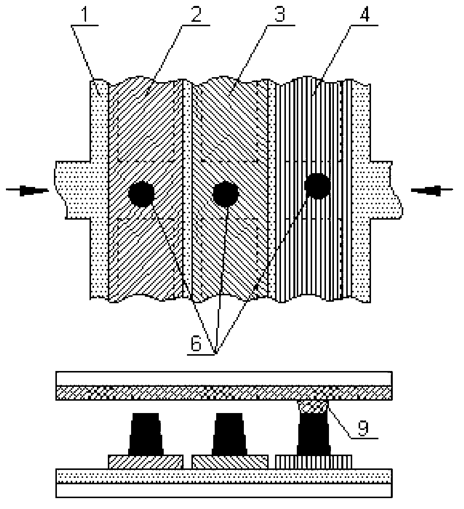
[0125] The difference between the manufacturing method of the color filter substrate in this embodiment and that in Embodiment 2 is that step 1 is slightly different.

[0126] In this embodiment, in step 1, the step of simultaneously forming the bottom pad during the process of forming the color film layer includes:

[0127] Step 11B: forming a first color film layer on the black matrix;

[0128] Step 12B: forming a second color film layer on the black matrix;

[0129] Step 13B: forming a third color film layer on the black matrix, and simultaneously forming a bottom pad on the first color film layer and the second color film layer. Wherein, the base pad and the third color film layer are simultaneously formed by the same mask plate through a patterning process, and the mask plate is formed by slightly improving the existing mask plate for making the color film layer.

[0130] Wherein, the bottom pad formed on the first color film layer and the bottom pad formed on the secon...


PUM

PropertyMeasurementUnit
heightaaaaaaaaaa

Abstract

The invention provides a color film substrate, a production method thereof and a liquid crystal panel with the color film substrate. The production method of the color film substrate includes the following steps: 1) base pads are arranged at design positions of spacers on a first substrate; 2) the spacers are respectively arranged on the base pads and at other design positions of the spacers without the base pads on the first substrate to form spacers with different heights; or the base pads have two or multiple different heights, and the spacers are respectively arranged on the base pads with the different heights to form the spacers with the different heights. By the production method, various height differences of the spacers can be formed, and production cost is low.

Description

technical field [0001] The invention belongs to the technical field of display manufacturing, and in particular relates to a color filter substrate, a manufacturing method thereof, and a liquid crystal panel including the color filter substrate. Background technique [0002] In the existing liquid crystal panel, a plurality of spacers are usually arranged between the color filter substrate and the array substrate, and the heights of the plurality of spacers are generally the same. figure 1 It shows the position diagram of the spacer (column spacer) commonly used in the prior art on the color filter substrate and the cross-sectional view of the liquid crystal panel formed by the color filter substrate after the cell alignment is completed. From figure 1 It can be seen that the heights of spacers commonly used at present are equal. However, with the further popularization and application of liquid crystal displays, in order to obtain a certain amount of liquid crystal fillin...

Claims


Application Information

Patent Timeline
Patent Type & Authority Applications(China)
IPC IPC(8): G02F1/1339G02F1/1335
CPCG02F1/133514G02F1/133516G02F1/13394G02F1/13396
Inventor 杨瑞智林准焕张俊瑞
Owner BOE TECH GRP CO LTD
Why Eureka
Try Eureka