Array substrate and display panel

A technology for array substrates and display panels, applied in static indicators, optics, instruments, etc., can solve the problems of reduced side light transmittance, poor curing effect of frame glue, etc.

Active Publication Date: 2013-09-04
XIAMEN TIANMA MICRO ELECTRONICS
View PDF4 Cites 8 Cited by
  • Summary
  • Abstract
  • Description
  • Claims
  • Application Information

AI Technical Summary

Problems solved by technology

[0006] An embodiment of the present invention provides an array substrate and a display panel, which are used to solve the problem of the lower light transmittance of the seal glue a...

Method used


Image

  • Array substrate and display panel
  • Array substrate and display panel
  • Array substrate and display panel

Examples


Embodiment Construction

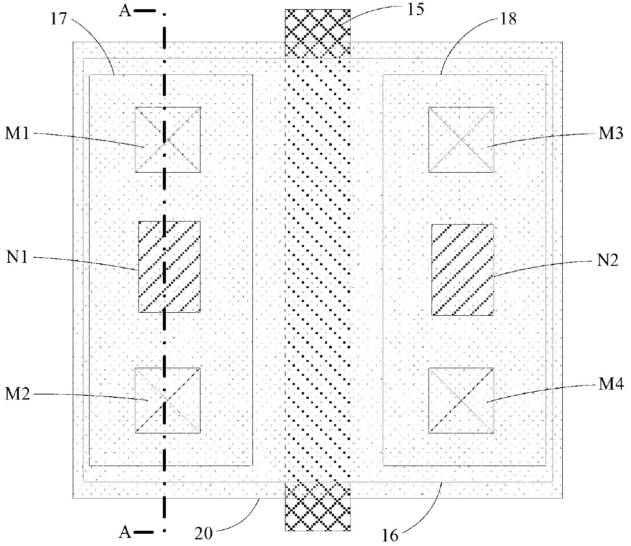
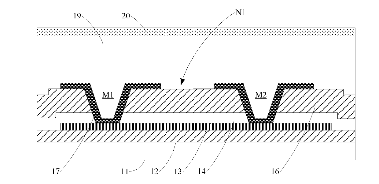
[0029] The driving circuit in the array substrate of the embodiment of the present invention includes at least one switch device connected to the signal line of the effective display area, the switch device includes a channel structure for providing a transmission channel for signals and adopts an opaque material, wherein the The channel structure has at least one light-transmitting part, through which external light can be emitted, thereby enhancing the light transmittance of the switch device without affecting the characteristics of the switch device.

[0030] Embodiments of the present invention will be further described in detail below in conjunction with the accompanying drawings.

[0031] The array substrate provided by the embodiment of the present invention includes an effective display area and a driving circuit arranged on the periphery of the effective display area. The driving circuit includes at least one switch device connected to the signal line in the effective ...


PUM


Abstract

The invention discloses an array substrate and a display panel and aims at solving the problem of the existing array substrate that the large density of TFT (Thin Film Transistor) elements in the region of a driving circuit results in the reduction of the light transitivity on the lower side of a sealant region and poor sealant curing effect. The array substrate in the embodiment of the invention comprises an effective display region and a driving circuit arranged on the periphery of the effective display region, wherein the driving circuit comprises at least one switch device which is connected with a signal wire of the effective display region, the switch device comprises a channel structure which is used for providing signals with a transmission channel and is made of an opaque material, and at least one light transmitting part is arranged on the channel structure. As at least one light transmitting part is arranged on the channel structure of the at least one switch device in the array substrate of the embodiment of the invention, the light transitivity of the switch device is increased.

Description

technical field [0001] The invention relates to the field of display panel manufacturing, in particular to an array substrate and a display panel. Background technique [0002] Liquid Crystal Display (LCD) has the characteristics of low power consumption, low radiation and low manufacturing cost, and has been widely used in various electronic devices, such as digital electronic devices such as display devices, TVs, mobile phones, and digital cameras. Among them, a low temperature polysilicon liquid crystal display device (LTPS LCD, Low Temperature Poly Silicon Liquid Crystal Display) is a mainstream product in the liquid crystal display device. [0003] see figure 1 As shown, it is a schematic structural diagram of an existing display panel (panel), and the display panel includes: an active display area (AA, Active Area) a, an area b where the driving circuit is located around the active display area a, and distributed in The sealant area c on the periphery of the effectiv...

Claims


Application Information

Patent Timeline
IPC IPC(8): G09G3/36H01L29/786H01L29/417G02F1/1368G02F1/1339
Inventor 吴昊夏军
Owner XIAMEN TIANMA MICRO ELECTRONICS
Why Eureka
Try Eureka