Binding equipment and binding method of chip

A chip and equipment technology, applied in the field of liquid crystal display equipment manufacturing process, can solve the problems of chip breakage, chip and substrate warpage, chip peeling, etc., to prevent warpage and reduce stress.

Inactive Publication Date: 2013-09-11
BEIJING BOE OPTOELECTRONCIS TECH CO LTD
View PDF6 Cites 15 Cited by
  • Summary
  • Abstract
  • Description
  • Claims
  • Application Information

AI Technical Summary

Problems solved by technology

After the anisotropic conductive adhesive is cured, the relative position between the chip and the substrate is fixed. After the main pressure is finished, the chip and the substrate cool down, and the shrinkage of the chip is larger than that of the substrate, so that the two ends of the chip have a larger opposition to the substrate. stress, which causes chip and substrate warpage
The warpage of the chip and the substrate will lead to adverse consequences such as chip peeling, chip breakage, and uneven brightness and darkness of the display effect.
[0004] At present, low-temperature anisotropic conductive adhesive products are mainly used to solve the problem of chip and substrate warpage, but the product is currently expensive and the technology is immature

Method used


Image

  • Binding equipment and binding method of chip
  • Binding equipment and binding method of chip
  • Binding equipment and binding method of chip

Examples


Embodiment Construction

[0033] The following will clearly and completely describe the technical solutions in the embodiments of the present invention with reference to the accompanying drawings in the embodiments of the present invention. Obviously, the described embodiments are some of the embodiments of the present invention, but not all of them. Based on the embodiments of the present invention, all other embodiments obtained by persons of ordinary skill in the art without making creative efforts belong to the protection scope of the present invention.

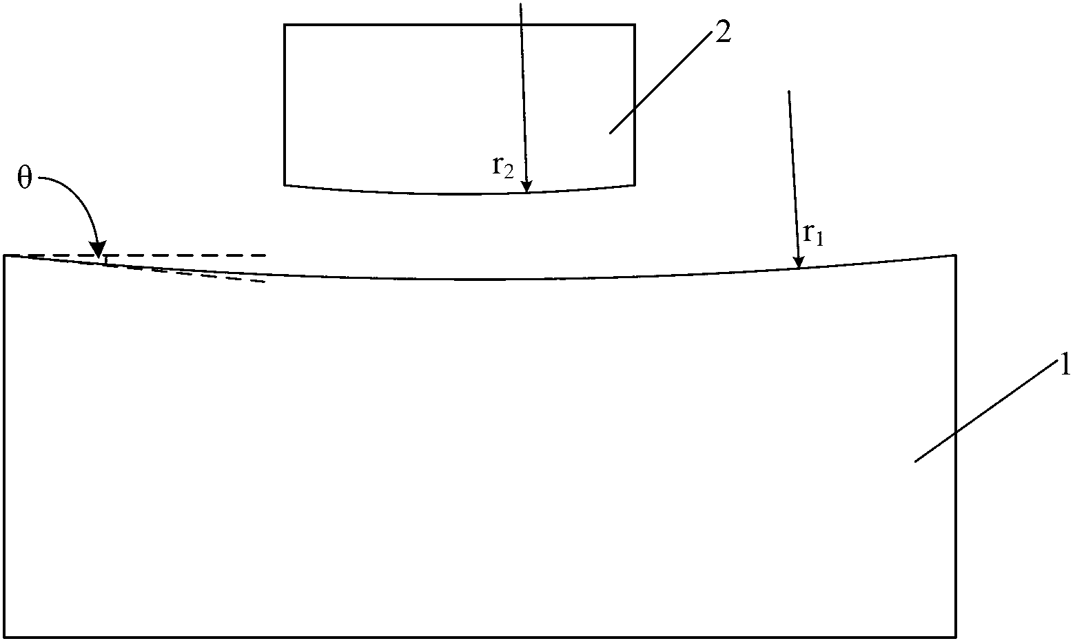
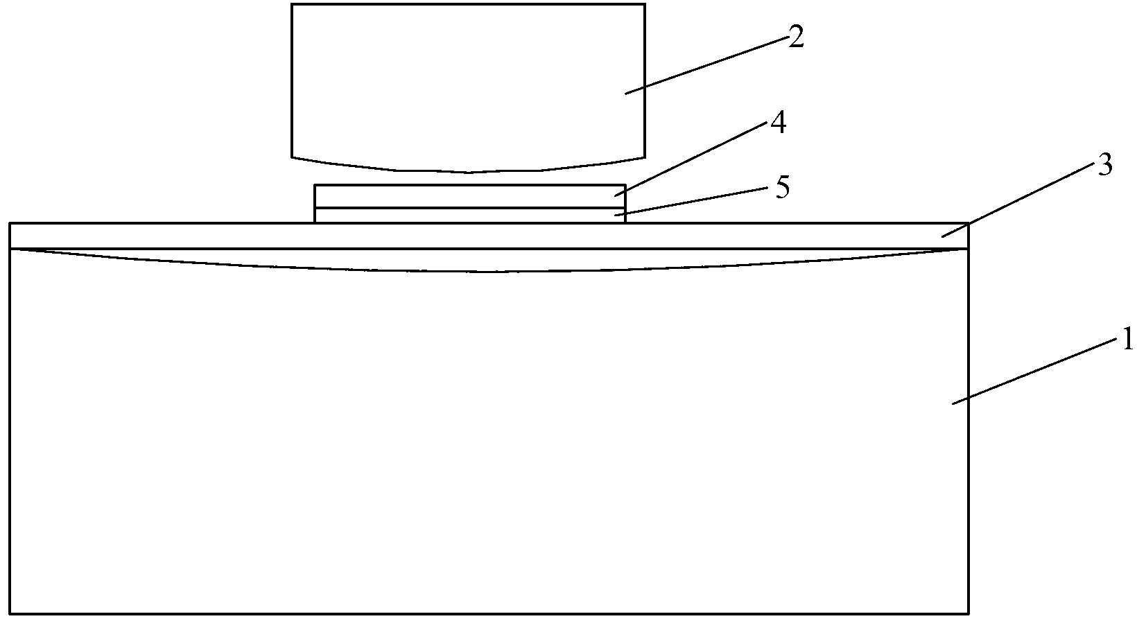
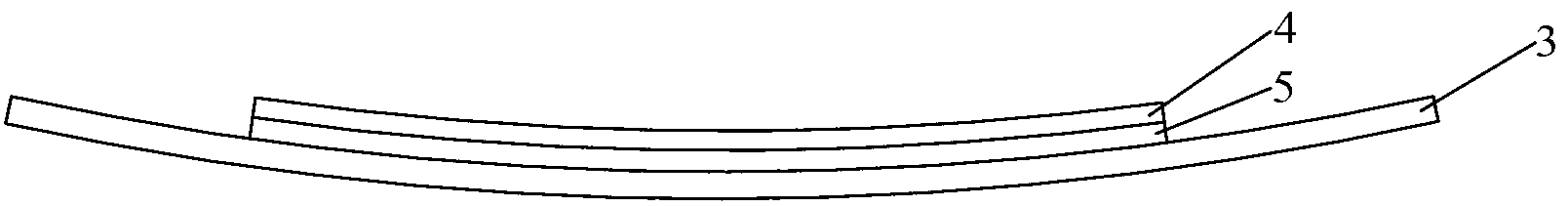
[0034] An embodiment of the present invention provides a chip binding device, such as figure 1 As shown, the bonding device of the chip includes a base 1 and an indenter 2,

[0035] The side of the base 1 for carrying the substrate has a first downward arc, the side of the indenter 2 and the chip has a second downward arc, the base 1 with the first arc and the base with the The indenter 2 of the second arc matches.

[0036] Such as figure 1 As ...


PUM


Abstract

An embodiment of the invention discloses binding equipment and a binding method of a chip, relates to the field of production technique of liquid crystal displaying equipment, and can solve the problem of warping after the chip and a substrate are bound. The binding equipment of the chip comprises a base platform and a pressure head, one surface, used for bearing a substrate, of the base platform has a first downward arc, one surface, in contact with the chip, of the pressure head has a second downward arc, and the base platform with the first arc is matched with the pressure head with the second arc.

Description

technical field [0001] The invention relates to the field of manufacturing technology of liquid crystal display devices, in particular to a chip binding device and method. Background technique [0002] In order to better reduce costs, the current small-size LCD products basically use the (Chip On Glass, COG for short) chip bonding process to drive the LCD panel. Specifically, after forming bumps on the bare chip, on the substrate Connect directly to the leads of the LCD screen. [0003] During the COG bonding process, when the main pressure is performed, the high-temperature indenter first contacts the chip, and the heat is conducted to the anisotropic conductive adhesive and the substrate through the chip. At this time, the temperature difference between the substrate and the platform is large, causing There is a difference in swell size between the two. After the anisotropic conductive adhesive is cured, the relative position between the chip and the substrate is fixed. ...

Claims


Application Information

Patent Timeline
IPC IPC(8): H01L21/67H01L21/603
CPCH01L24/75H01L2924/3511H01L2224/29299H01L2224/75983H01L24/29H01L24/32H01L2224/2929H01L2224/32225H01L2224/83193H01L2224/83203H01L2924/07811H01L2924/15788H01L24/83H01L25/50H01L25/04H01L2924/20105H01L2924/00014H01L25/0655H01L2224/83192H01L2224/8385
Inventor 李瑞权宁万宋勇
Owner BEIJING BOE OPTOELECTRONCIS TECH CO LTD
Why Eureka
Try Eureka