Splitting device

A technology of cleavage and dicing, which is applied in the field of cleavage devices for cleavage of semiconductors, which can solve the problems of time-consuming and labor-intensive operation, wear samples, cumbersome processes, etc., and achieve the effects of avoiding damage, improving quality, and improving process efficiency

Active Publication Date: 2013-09-11
SUZHOU INST OF NANO TECH & NANO BIONICS CHINESE ACEDEMY OF SCI
View PDF5 Cites 7 Cited by
  • Summary
  • Abstract
  • Description
  • Claims
  • Application Information

AI Technical Summary

Problems solved by technology

However, this protection process will also bring cumbersome and difficult processes, such as the removal of the protective glue after cleavage. Since the sample becomes smaller, the cleaning process will also wear the sample, and the operation is time-consuming and laborious.

Method used


Image

  • Splitting device
  • Splitting device
  • Splitting device

Examples


Embodiment 1

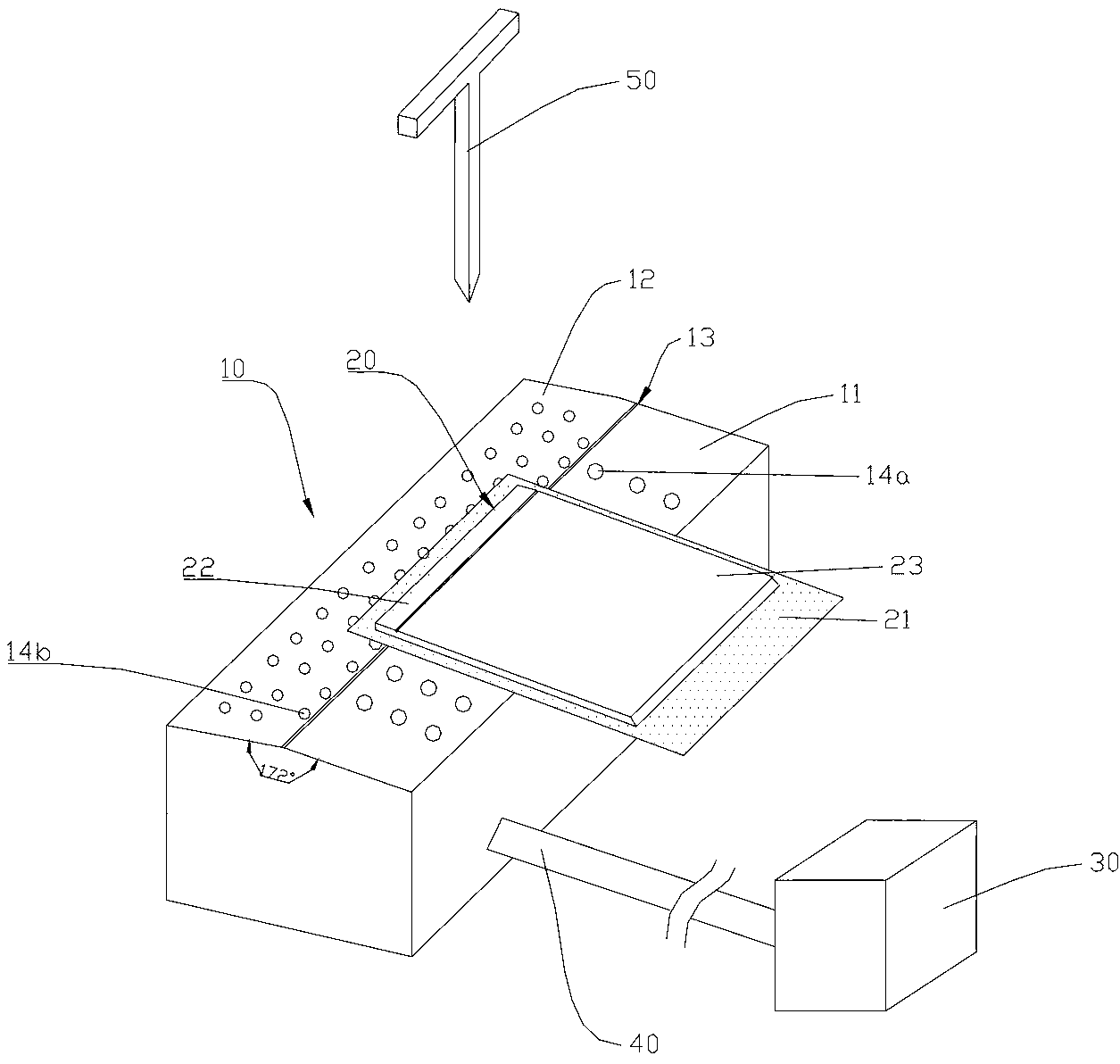
[0023] This embodiment provides a cleavage device for realizing the natural cleavage of bars into chips. Wherein, in order to illustrate the feature of the present invention more clearly, define: each bar comprises two parts, and a part of dicing is the part to be cleaved as the quasi-chip, and the remaining part is the bar to be cleaved. The thickness of the bars in this embodiment is 70-150 μm, and the width of a cut chip is about 500 μm.

[0024] Such as figure 1 As shown, the cleavage device provided in this embodiment includes:

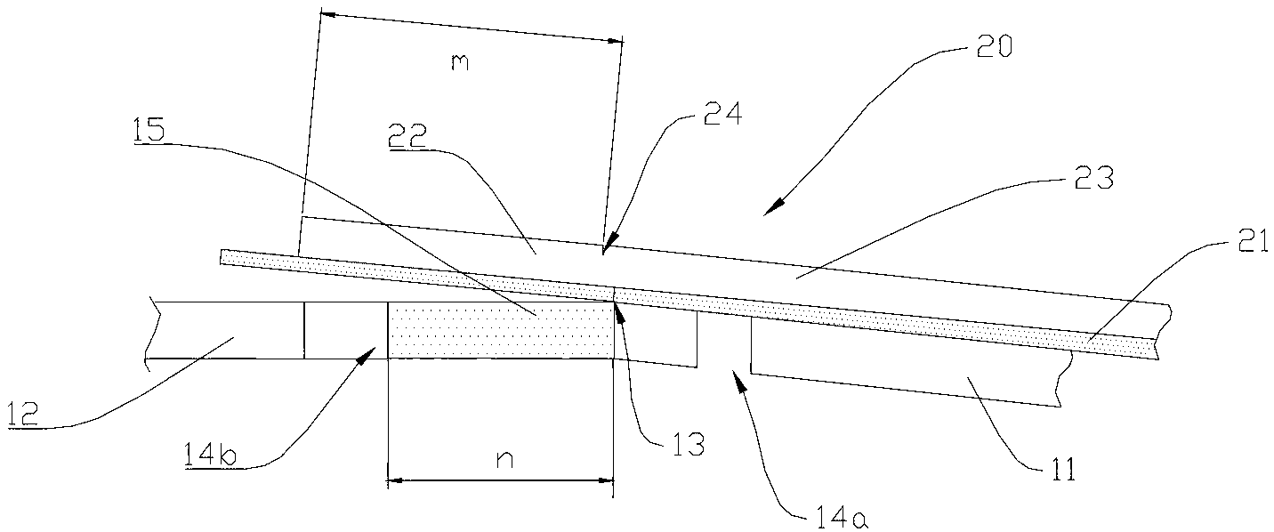
[0025] The cuboid adsorption cavity 10 is provided with a first upper cover 11 and a second upper cover 12 on its top. The second upper cover 12 is arranged horizontally parallel to the bottom of the adsorption cavity 10 , and the first upper cover 11 and the second upper cover 12 support each other at an included angle (172°) to form a ridge 13 after tilting. Wherein, the ridge 13 is used to straddle the bar 20 above it as a fulcrum for cleav...

Embodiment 2

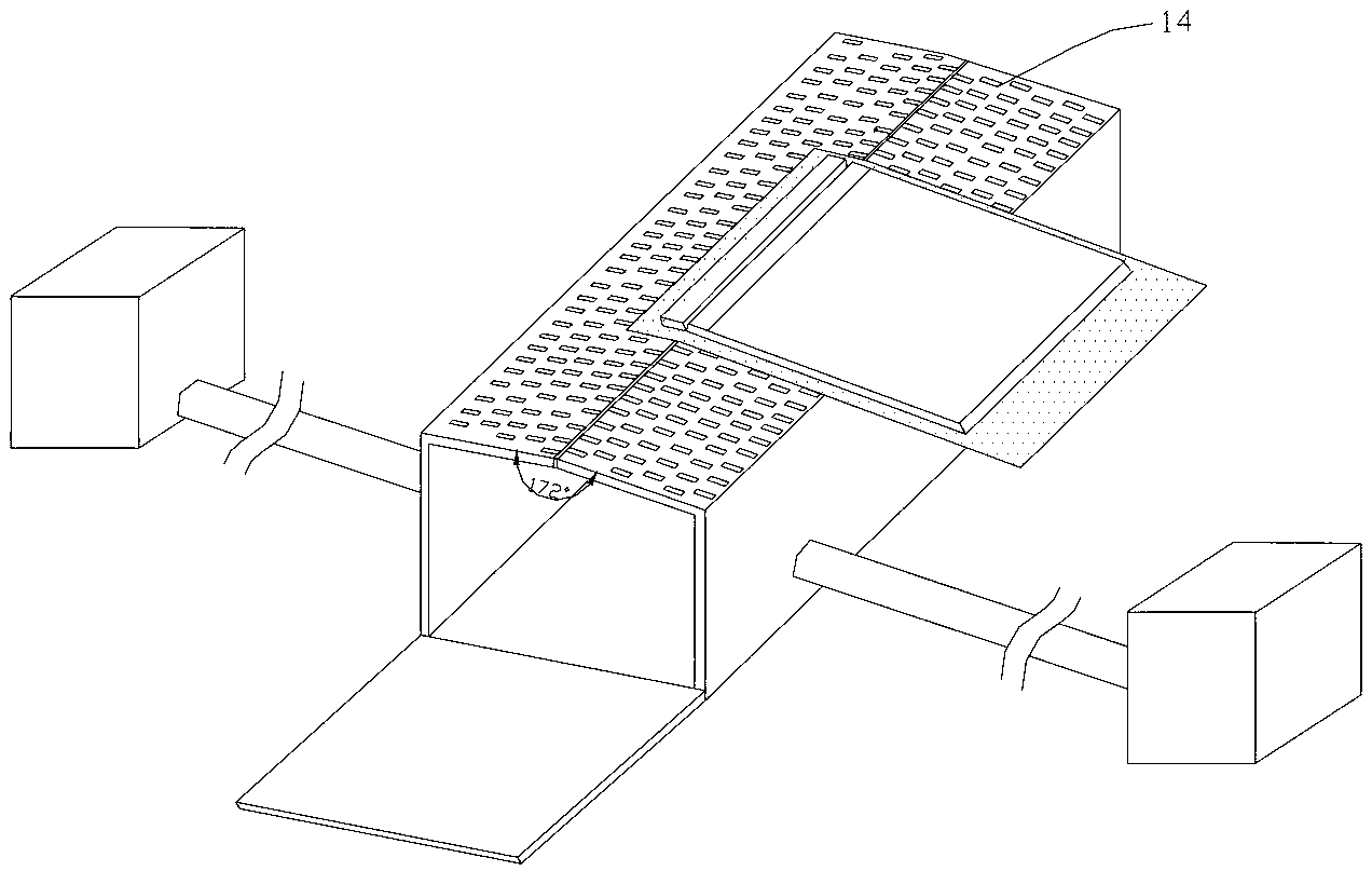
[0051] This embodiment is improved on the basis of Embodiment 1, especially for some bars with a larger thickness (150-400 μm), it can be better cleaved. like Figure 5 As shown in (a), the adsorption chamber 10 of this embodiment also has holes 16 on the scribing table 15 . Corresponding to the bottom of the scribing table 15, a support assembly 60 is provided in the adsorption cavity 10 for passing through the holes 16 opened on the scribing table 15 to apply the adsorption force to the bar 20 Support forces in the opposite direction. In order to avoid affecting the stability of dicing, the width of the hole groove 16 can be no more than 1 / 2 of the scribing table 15, for example, corresponding to a chip with a width of 500 μm, and the dicing table 15 is set to 400 μm, then the width of the hole groove 16 will be No more than 200μm. However, the width and shape of the hole 16 are not limited, and can be adjusted according to the shape of the actual support assembly 60 . T...


PUM


Abstract

The invention relates to the preparation technology of semiconductors, in particular to a splitting device. The splitting device is used for splitting a semiconductor bar into multiple chips. The splitting device comprises a negative pressure source and an absorbing cavity which is connected with the negative pressure source through a connecting pipe. The absorbing cavity comprises a first upper cover and a second upper cover. The first upper cover and the second upper cover are mutually supported in a way of an included angle to form a ridge. A plurality of through holes are formed in each of the first upper cover and the second upper cover. The through holes correspond to the bar spans on the first upper cover and the second upper cover. The bar is naturally split by using the ridge as a support point and through the absorbing force of the absorbing cavity to the bar. By the absorbing force, noncontact splitting of chip structural faces is achieved, sample surface structure can be protected from being damaged, and yield can be increased.

Description

technical field [0001] The invention relates to the technical field of semiconductor materials, in particular to a cleaving device for cleaving semiconductors. Background technique [0002] At present, the cleavage process of optoelectronic devices (such as bars) made of materials such as GaAs and InP generally uses a diamond knife to cut a gap and then rolls on the bar with a roller, and applies downward pressure to the bar to crack the bar. open effect. This method of cleavage will cause a greater degree of mechanical damage to some samples whose surface structure is not resistant to pressure. At the same time, the roller directly contacts the surface of the chip structure, and the debris generated by the lobes is easy to adhere to the roller. It brings a certain degree of debris and the possibility of contaminating the surface of the sample structure. [0003] In order to avoid the above damage, the existing process protects the surface of the sample before cleavage, su...

Claims


Application Information

Patent Timeline
Patent Type & Authority Applications(China)
IPC IPC(8): H01S5/02
Inventor 黄宏娟赵德胜张宝顺
Owner SUZHOU INST OF NANO TECH & NANO BIONICS CHINESE ACEDEMY OF SCI
Why Eureka
Try Eureka