

High-frequency module
A high-frequency module and high-frequency signal technology, which is applied to semiconductor/solid-state device components, semiconductor devices, electrical components, etc., can solve the problem of inappropriate thinning of high-frequency modules, and achieve the effect of reducing cost and reducing processes
- Summary
- Abstract
- Description
- Claims
- Application Information
AI Technical Summary
Problems solved by technology
Method used
Image

Examples
no. 1 approach )
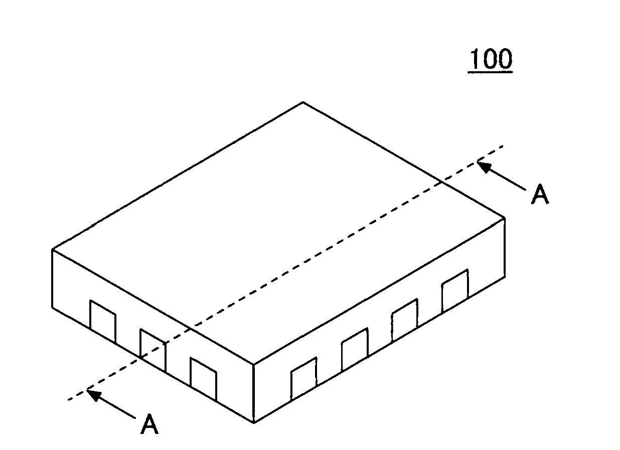
[0047] Hereinafter, a first embodiment of the present invention will be described with reference to the drawings. figure 1 It is a figure explaining the high frequency module of 1st Embodiment.
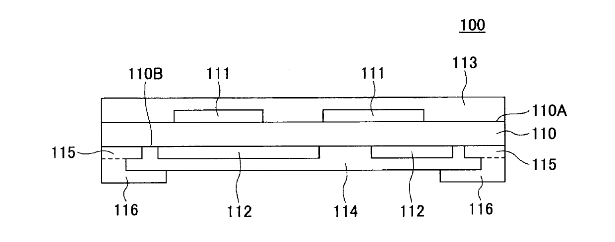
[0048] The high-frequency module 100 of the present embodiment is configured by sealing electronic components mounted on a circuit board with resin or the like. The high-frequency module 100 of the present embodiment is mounted on a communication device that performs wireless communication, for example, a wireless LAN (Local Area Network) device, a 1seg tuner device, a GPS (Global Positioning System) device, and the like. figure 2 It is the A-A sectional view of the high-frequency module.
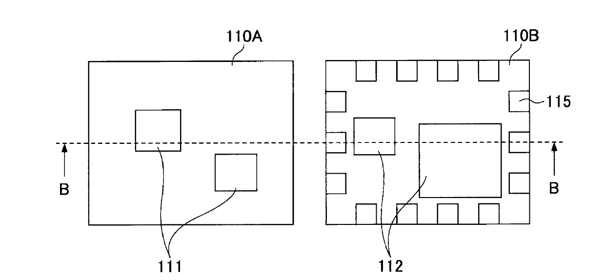
[0049] In the high-frequency module 100 of this embodiment, electronic components 111 and 112 are respectively mounted on one surface 110A and the other surface 110B of the circuit board 110 . The circuit board 110 of the present embodiment is formed of, for example, ceramics or epoxy resin. Fu...
no. 2 approach )
[0060] Hereinafter, a second embodiment of the present invention will be described with reference to the drawings. The second embodiment of the present invention differs from the first embodiment only in that electrodes for leading out terminals 115 to the surface of resin mold layer 114 are mounted on a substrate in advance. Therefore, in the following description of the second embodiment, components having the same functional configuration as those of the first embodiment are given the same reference numerals as those used in the description of the first embodiment, and descriptions thereof are omitted.
[0061] Figure 5A to Figure 5C It is a figure explaining the manufacturing method of the high frequency module of 2nd Embodiment. In the high-frequency module 100A of the present embodiment, a member to be an electrode member 116A is preliminarily mounted on a substrate 110 .
[0062] Such as Figure 5A As shown, electrode member 116A is attached to the position where te...
no. 3 approach )
[0074] Hereinafter, a third embodiment of the present invention will be described with reference to the drawings. The third embodiment of the present invention differs from the first embodiment in that a high-frequency module and an antenna are integrally formed. Therefore, in the following description of the third embodiment, components having the same functional configuration as those of the first embodiment are given the same reference numerals as those used in the description of the first embodiment, and descriptions thereof are omitted. .
[0075] Figure 7 It is the 1st figure explaining the high frequency module of 3rd Embodiment. Figure 7 In the illustrated high-frequency module 100B, an antenna 119 and a surface pattern 120 for connecting the terminal 115 and the antenna 119 are formed on the surface of the resin mold layer 113 .
[0076] In addition, in Figure 7 Although the example in which the antenna 119 and the surface pattern 120 are formed on the high fre...
PUM
 Abstract
Description
Claims
Application Information