
SRAM timing sequence test circuit and test method

A technology for timing testing and testing circuits, applied in static memory, instruments, etc., can solve the problems of uncontrollable accuracy, time-consuming, and uncertainty of Tcq measurement, saving time for selection and adjustment, simple measurement, and small error. Effect

Active Publication Date: 2013-09-25
SUZHOU ZHAOXIN SEMICON TECH CO LTD
View PDF3 Cites 18 Cited by
  • Summary
  • Abstract
  • Description
  • Claims
  • Application Information

AI Technical Summary

Problems solved by technology

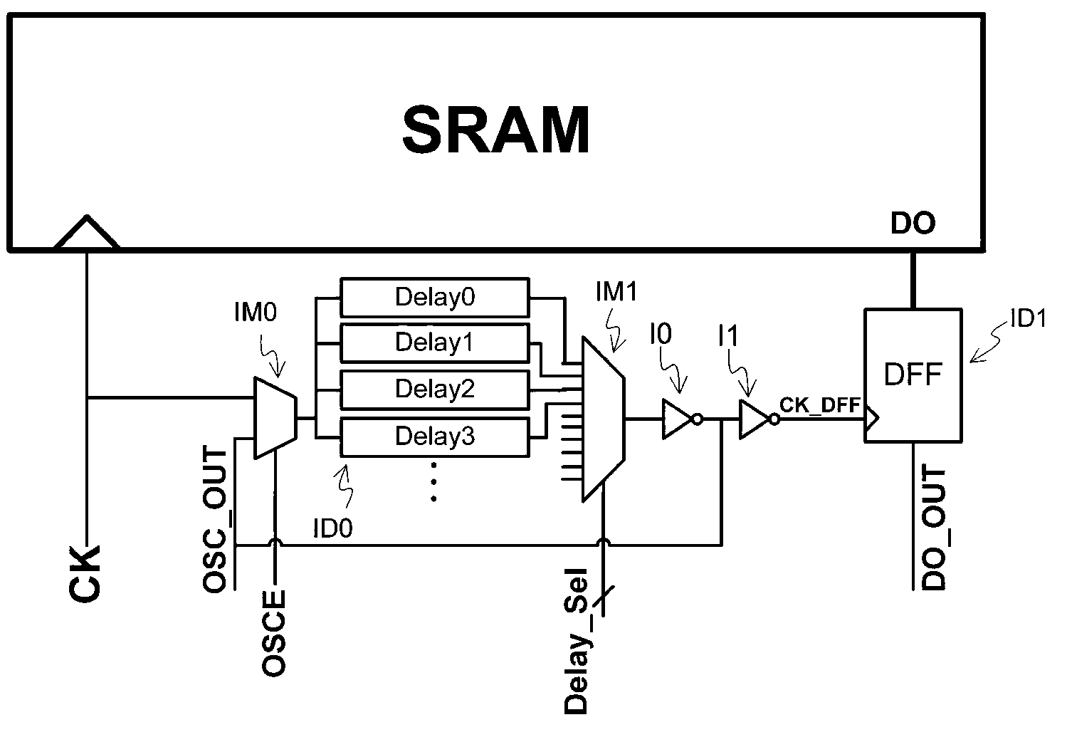
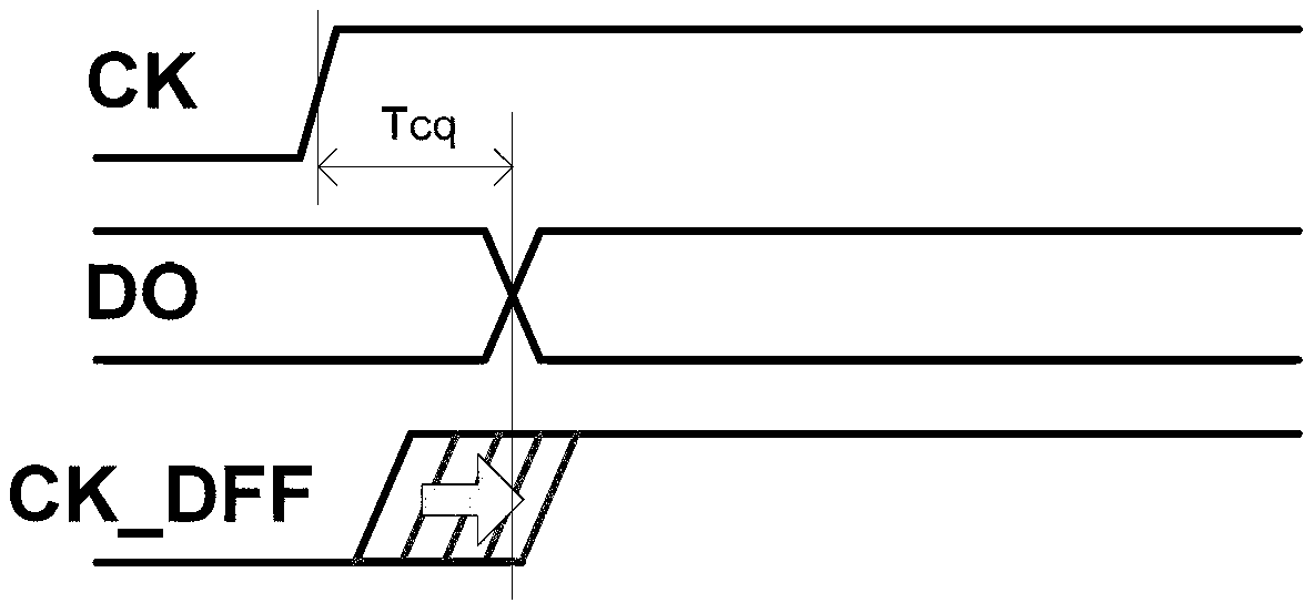
[0005] However, the disadvantages of this circuit are: (1) It involves more manual layout design, which consumes more time and is less efficient. For example, in order to ensure the accuracy of Tcq measurement, the delay circuit ID0 needs to be completed manually, otherwise it will be generated by automatic layout and routing tools. The circuit layout delay has great uncertainty, which causes the accuracy of Tcq measurement to be uncontrollable; (2) The accuracy of Tcq measurement is low. For example, the measurement of Tcq by delay unit Delay1 fails, but the measurement of Tcq by delay unit Delay2 succeeds, then Tcq Between the delay time of Delay1 and the delay time of Delay2, the minimum measurement error is the difference between the two delay times; (3) The process of measuring Tcq is cumbersome, and it is necessary to continuously adjust Delay_Sel until the output data of the SRAM is correctly latched

Method used


Image

  • SRAM timing sequence test circuit and test method
  • SRAM timing sequence test circuit and test method
  • SRAM timing sequence test circuit and test method

Examples


Embodiment Construction

[0036] The technical solutions of the embodiments of the present invention will be clearly and completely described below in conjunction with the accompanying drawings of the present invention.

[0037] A SRAM timing test circuit disclosed by the present invention, by forming two ring oscillation circuits, respectively measuring the output oscillation periods of the two ring oscillation circuits, thereby accurately obtaining the time value of the SRAM storage unit reading data, to overcome the existing Tcq The measurement method has the problems of low measurement accuracy, cumbersome process, time-consuming and low efficiency.

[0038] Such as Figure 4 As shown, a SRAM timing test circuit disclosed in the present invention includes: SRAM storage unit I10, a first mode switching circuit I5, an edge signal trigger circuit, a second mode switching circuit I8, an address generating circuit I9 and a third mode switching circuit I11, the SRAM storage unit I10 is a clock synchroniza...


PUM


Abstract

The invention discloses a SRAM timing sequence test circuit and a test method. The test circuit comprises a SRAM memory cell and a test circuit unit. The test circuit unit comprises a first mode switching circuit connected with the SRAM memory cell, an edge signal trigger circuit connected with the first mode switching circuit and a second mode switching circuit connected with the edge signal trigger circuit. The first mode switching circuit has a first enable pin. The second mode switching circuit has a second enable pin. According to signal control difference of the first and second enable pins, a first annular oscillating circuit and a second annular oscillating circuit are respectively formed in the test circuit; and output oscillation periods of the two annular oscillating circuits are measured so as to accurately obtain time value of reading data of the SRAM memory cell. The test circuit provided by the invention can be completed by an automatic wiring tool, and has advantages of small measuring error, high precision and simple measurement.

Description

technical field [0001] The invention relates to the unit circuit field of a static random access memory (SRAM), in particular to a timing test circuit and a testing method for testing timing index parameters of the SRAM. Background technique [0002] After the semiconductor technology enters the deep sub-micron era, the chip can work at a frequency of several hundred MHz or upper GHz, and the working frequency of its internal SRAM may be higher. However, in chip testing, due to the impact of packaging and testing equipment, the clock signal provided by external testing can only reach a frequency of tens or at most 100 MHz. [0003] In the aforementioned context, today's chip testing generally relies heavily on built-in self-test (BIST) circuits. The advantage of BIST circuits is not only the automation of testing, but also high-speed testing because no external testing paths are required. The BIST circuit of the SRAM is also called the memory built-in self-test (MBIST) circ...

Claims


Application Information

Patent Timeline
Patent Type & Authority Applications(China)
IPC IPC(8): G11C29/08
Inventor 王林
Owner SUZHOU ZHAOXIN SEMICON TECH CO LTD
Learn More