Buried resistor and manufacture process thereof

A technology of manufacturing process and embedded resistors, which is applied in the direction of assembling printed circuits with electrical components, printed circuits connected with non-printed electrical components, etc. problems, to achieve the effect of improving production efficiency and product quality, reducing the number of SMT solder joints, and improving reliability

Active Publication Date: 2013-10-02
苏州市三生电子有限公司
View PDF6 Cites 8 Cited by
  • Summary
  • Abstract
  • Description
  • Claims
  • Application Information

AI Technical Summary

Problems solved by technology

[0003] Buried resistor materials are widely used, and almost all multilayer boards can be used. However, now the buried resistor is still in the promotion stage, and PCB manufacturers do not have suitable matching technology and equipment for the time being, so the buried resistor is only used. in the high-tech field

Method used


Image

  • Buried resistor and manufacture process thereof

Examples


Embodiment 1

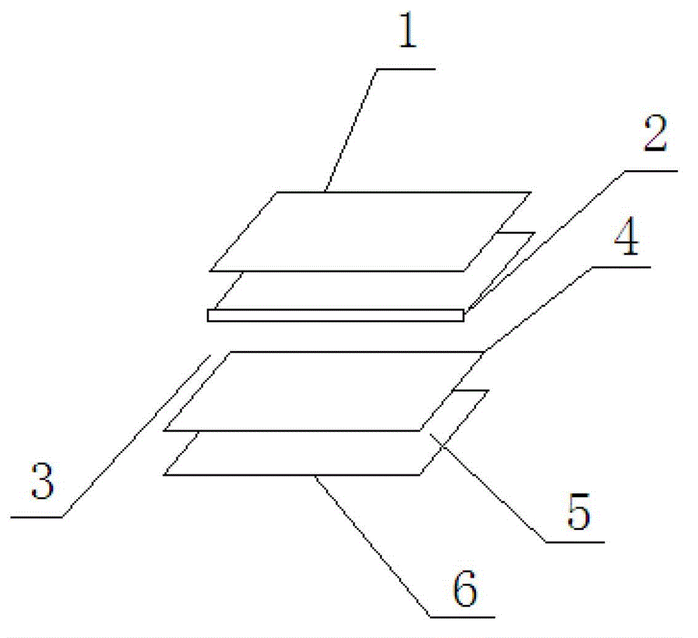
[0032] like figure 1 As shown, a buried resistor includes: the first layer of copper foil layer 1, the second layer of copper foil layer 4, the third layer of copper foil layer 6, the first layer of insulating PP layer 3, the second layer of insulating PP layer 5, The insulating base layer and the resistance layer 2, the third layer of copper foil layer 6, the second layer of insulating PP layer 5, the second layer of copper foil layer 4, the first layer of insulating PP layer 3, the resistance layer 2, the first layer of copper foil Layer 1 is sequentially arranged on the insulating base layer from bottom to top, and a resistance layer 2 is arranged between the first layer of copper foil layer 1 and the first insulating PP layer 3, and between the first insulating PP layer 3 and the second insulating PP layer 5 A second layer of copper foil layer 4 is arranged between them, and a third layer of copper foil layer 6 is arranged between the second layer of copper foil layer 4 a...

Embodiment 2

[0048] like figure 1 As shown, a buried resistor includes: the first layer of copper foil layer 1, the second layer of copper foil layer 4, the third layer of copper foil layer 6, the first layer of insulating PP layer 3, the second layer of insulating PP layer 5, The insulating base layer and the resistance layer 2, the third layer of copper foil layer 6, the second layer of insulating PP layer 5, the second layer of copper foil layer 4, the first layer of insulating PP layer 3, the resistance layer 2, the first layer of copper foil Layer 1 is sequentially arranged on the insulating base layer from bottom to top, and a resistance layer 2 is arranged between the first layer of copper foil layer 1 and the first insulating PP layer 3, and between the first insulating PP layer 3 and the second insulating PP layer 5 A second layer of copper foil layer 4 is arranged between them, and a third layer of copper foil layer 6 is arranged between the second layer of copper foil layer 4 a...


PUM


Abstract

The invention relates to the buried resistor technical field, in particular to a buried resistor and a manufacture process thereof. The buried resistor includes a first copper foil layer, a second copper foil layer, a third copper foil layer, a first insulating PP layer, a second insulating PP layer, an insulating base layer and a resistance layer, wherein the third copper foil layer, the second insulating PP layer, the second copper foil layer, the first insulating PP layer, the resistance layer and the first copper foil layer are sequentially arranged on the insulating base layer from bottom to up, the resistance layer is arranged between the first copper foil layer and the first insulating PP layer, the second copper foil layer is arranged between the first insulating PP layer and the second insulating PP layer, and the third copper foil layer is arranged between the second copper foil layer and the insulating base layer. An ultrathin core board is machined through using a double-sided etching one-step lamination method so as to form a buried resistor structure, and therefore, production efficiency is greatly improved, and product quality can be ensured; and with the buried resistor applied to a PCB, the space of the PCB can be saved, and at the same time, the reliability of the PCB can be improved.

Description

Technical field [0001] The invention involves the field of buried resistance technology, and specially involves a buried resistance and its manufacturing process. Background technique [0002] The so -called buried resistor, also known as buried resistance, is to press the special resistance material on the insulating substrate, and then use printing, etching and other processes to form the inner (outer) material of the required resistance value required for the design, and then press it on the PCB board.Inner (top), a technology of a flat resistance layer. [0003] The application of resistance materials is widely used, and almost all multi -layer boards can be used, but now the main reasoning resistance is only staying in the promotion stage. In addition, PCB manufacturers have no compatible supporting technology and equipment for the time being, so only the burial resistance is only used to use only useIn the field of high -tech. Invention content [0004] The purpose of the ...

Claims


Application Information

Patent Timeline
Patent Type & Authority Applications(China)
IPC IPC(8): H05K1/18H05K3/30
Inventor 汪海洋巴超
Owner 苏州市三生电子有限公司
Why Eureka
Try Eureka