

Precise optical element one-step forming processing device and its process
A technology of precision optics and molding processing, which is applied in glass molding, glass reshaping, manufacturing tools, etc. It can solve the problems of failure in the production of precision optical components, increase the burden and pressure of enterprises, and limit the growth and development of enterprises, so as to avoid processing Effects of failure, promotion, smooth operation of equipment
- Summary
- Abstract
- Description
- Claims
- Application Information
AI Technical Summary
Problems solved by technology
Method used
Image

Examples
Embodiment 1
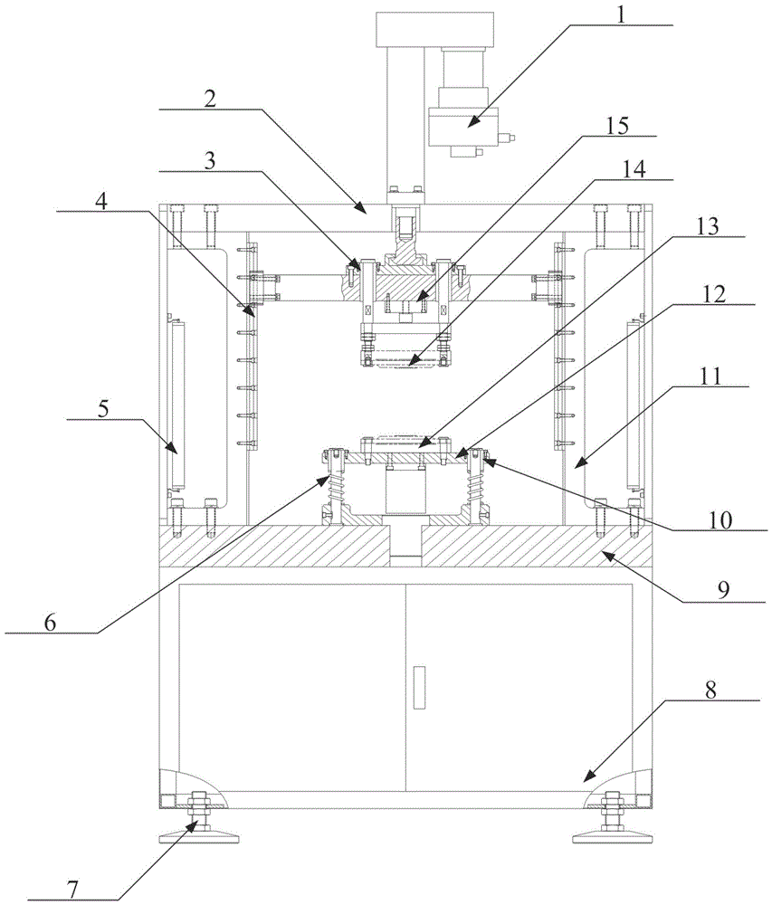
[0036] Such as figure 1 As shown, the precision optical element one-time molding processing device includes a frame 8, an adjustable support foot 7 is arranged at the lower end of the frame 8, a workbench 9 is arranged at the upper end of the frame 8, and a workbench 9 is also arranged on the workbench 9. A lower mold device and a column 11 are provided, and an upper support plate 2 is arranged on the top of the column 11. An upper mold device and a servo electric cylinder 1 are also arranged on the upper support plate 2. At the same time, the servo electric cylinder 1 is also connected There is a control cabinet.
[0037] Above-mentioned lower mold device comprises lower floating support frame 12, and this lower floating support frame 12 is provided with the support bar that is fixed on the workbench 9, and this support bar is covered with spring 6, and between the lower floating support frame 12 and the support bar A lower linear bearing 10 is provided, and a mold lower mol...
PUM
 Abstract
Description
Claims
Application Information