Supercharge Your Innovation With Domain-Expert AI Agents!

Trench preparation method

A trench and barrier layer technology, applied in the field of trench preparation, can solve the problems of integrated circuit damage, influence on integrated circuit performance, poor coverage, etc., and achieve the effect of avoiding damage

Active Publication Date: 2015-06-10
SEMICON MFG INT (SHANGHAI) CORP
View PDF3 Cites 0 Cited by
  • Summary
  • Abstract
  • Description
  • Claims
  • Application Information

AI Technical Summary

Problems solved by technology

[0008] Due to the existence of the gap 8, the second barrier layer 4 will not cover the lower interlayer dielectric layer 3 tightly, so that when the interconnection 7 is prepared later, metal materials (such as copper) will be filled in the gap 8, thereby A short connection is likely to occur between the metal materials filled in the gap 8 by the interconnection line 7, which will affect the performance of the integrated circuit and even cause the integrated circuit to be damaged.

Method used


Image

  • Trench preparation method
  • Trench preparation method
  • Trench preparation method

Examples


Embodiment Construction

[0041] In order to make the object, technical solution and advantages of the present invention clearer, the present invention will be further described in detail below with reference to the accompanying drawings and examples.

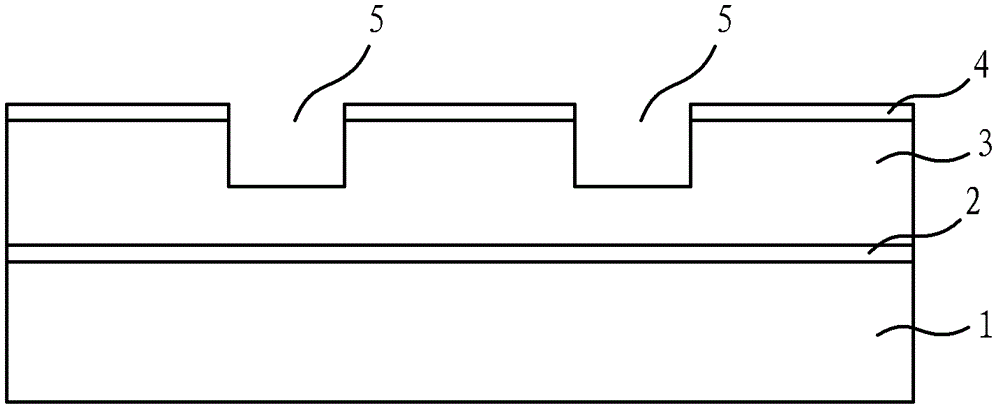
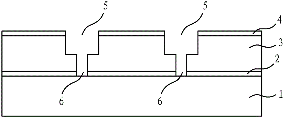
[0042] Such as Image 6 Shown is the flow chart of the steps of the groove preparation method of the present invention, Figure 7 to Figure 12 for corresponding to Image 6 The evolution diagram of the device structure at each step in the process, the following combination Image 6 as well as Figure 7 to Figure 12 The trench preparation method of the present invention is introduced in detail, including the preparation of through holes. The method mainly includes:

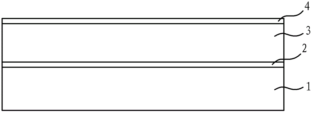
[0043] Step 1: A semiconductor device 1 is provided, and a first barrier layer 2, an interlayer dielectric layer 3, a second barrier layer 4 and a metal mask layer 9 are sequentially deposited on the semiconductor device 1, referring to Figure 7 shown.

[0044] Among them, the semicon...


PUM


Abstract

The invention discloses a trench preparation method in an IC (integrated circuit) interconnection preparation process. The method comprises the following steps: a semiconductor device is provided, wherein a first barrier layer, an interlayer dielectric layer, a second barrier layer and a metal mask layer are in order deposited on the semiconductor device; photoresist is coated on the metal mask layer and a graphical operation is carried out to the trench, and the photoresist serves as a mask to remove the metal mask layer and the second barrier layer and the photoresist is removed; a mask side wall is formed at the metal mask layer and a side wall of the second barrier layer; and a structure formed by previous steps is provided with the trench in the interlayer dielectric layer, and the mask side wall is simultaneously removed. In the invention, before the trench is formed, the mask side wall protects the interface between the side wall of the second barrier layer and the interlayer dielectric layer; and then the prepared interconnection material cannot be filled between the second barrier layer and the interlayer dielectric layer, so that the possible damage to the integrated circuit is prevented.

Description

technical field [0001] The invention relates to semiconductor manufacturing technology, in particular to a method for preparing grooves in the process of preparing IC interconnection lines. Background technique [0002] At present, in the production process of IC (Integrated Circuit, integrated circuit), when the interconnection (interconnection) is prepared, it is necessary to prepare trenches (Trench) and via holes (Via). Figure 1 to Figure 4 , to briefly introduce the preparation process of the internal connection. [0003] Such as figure 1 As shown, firstly, a fabricated semiconductor device 1 is provided, such as a MOS transistor, and a first barrier layer 2 , an interlayer dielectric layer 3 and a second barrier layer 4 are sequentially deposited on the surface of the semiconductor device 1 . [0004] Afterwards, the second barrier layer 4 and part of the interlayer dielectric layer 3 are etched using a patterned photoresist to form a trench 5, such as figure 2 sh...

Claims


Application Information

Patent Timeline
Patent Type & Authority Patents(China)
IPC IPC(8): H01L21/762
Inventor 邓浩
Owner SEMICON MFG INT (SHANGHAI) CORP
Features
  • R&D
  • Intellectual Property
  • Life Sciences
  • Materials
  • Tech Scout
  • Unparalleled Data Quality
  • Higher Quality Content
  • 60% Fewer Hallucinations
Learn More