

Chip testing method and chip
A technology of chip testing and testing signals, which is applied in the direction of electronic circuit testing, measuring electronics, measuring devices, etc., can solve the problems of increased chip production costs, waste of resources, and inability to make full use of pin resources, so as to reduce testing costs and improve testing efficiency effect
- Summary
- Abstract
- Description
- Claims
- Application Information
AI Technical Summary
Problems solved by technology
Method used
Image

Examples
Embodiment 1
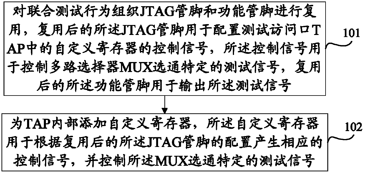
[0024] This embodiment provides a chip testing method, such as figure 1 As shown, the method includes:
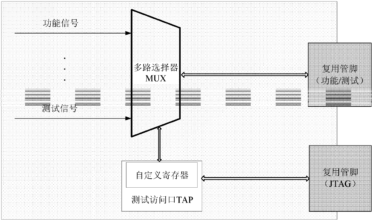
[0025] 101. Multiplexing the JTAG pins and functional pins of the joint test behavior organization, the multiplexed JTAG pins are used to configure the control signals of the custom registers in the test access port TAP, and the control signals are used to control The multiplexer MUX gates a specific test signal, and the multiplexed functional pins are used to output the test signal.
[0026] Optionally, while executing step 101, it also includes:
[0027] 102. Add a custom register inside the TAP, where the custom register is used to generate corresponding control signals according to the configuration of the multiplexed JTAG pins, and control the MUX to gate specific test signals. It should be noted that there is no strict execution order for steps 101 and 102, and they can be executed simultaneously or sequentially.
[0028] Optionally, after step 101 and step 102 are...
Embodiment 2
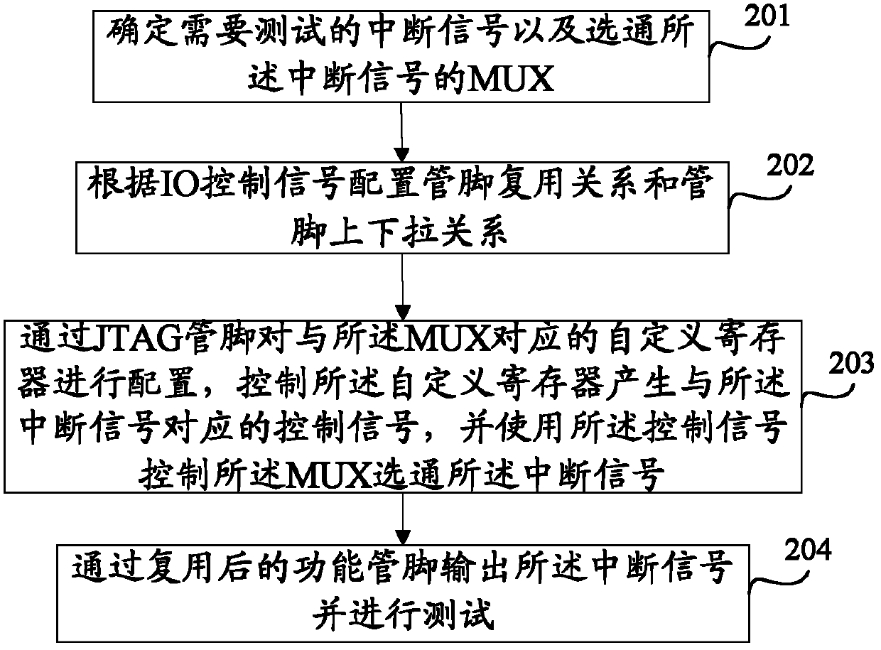
[0035] The present embodiment provides a kind of chip testing method, is example with the test of the interrupt signal of Watcgdog (watchdog) module and reset signal, as image 3 As shown, the method includes:
[0036] 201. Determine an interrupt signal to be tested and select a MUX for the interrupt signal.
[0037] Optionally, it can also be a reset signal. After the signal to be tested is determined, the custom register control signal corresponding to the test signal can be found according to the signal comparison table of the test signal and the control signal.
[0038] It should be noted that the interrupt signal and reset signal are mainly used to reset the system when the software runs away. The process is to send an interrupt notification first and then reset. In order to verify the integrity of the reset mechanism of the entire system, it is first necessary to confirm whether the Watcgdog module is correctly issued. The interrupt signal and reset signal are provided,...
Embodiment 3
[0052] This embodiment provides a chip testing method. When the test signal output by the chip through the pins is abnormal, locate the abnormal position, such as verifying the output signal PWM OUT1 of the PWM (Pulse Width Modulation, pulse width modulation) module, Lead the output signal PWMOUT1 of the PWM module to the input port of one of the MUX, such as Figure 5 As shown, the method includes:
[0053] 301. Determine a PWM OUT1 signal to be tested and a MUX for gating the PWM OUT1 signal.
[0054] Optionally, after the signal to be tested is determined, the custom register control signal corresponding to the test signal can be found according to the signal comparison table of the test signal and the control signal.
[0055] Wherein, before the PWM OUT1 signal of the test is determined, it also includes: multiplexing the JTAG pins and function pins, and the multiplexed JTAG pins are used to configure the custom registers in the test access port TAP A control signal, the...
PUM
 Abstract
Description
Claims
Application Information