
Semiconductor process monitoring method based on integrated leaning modeling technology

A technology of integrated learning and process monitoring, applied in the direction of electrical program control, comprehensive factory control, etc., can solve the problems of failing to meet the monitoring requirements of the semiconductor industry, and achieve the effect of improving the monitoring effect and improving the robustness

Inactive Publication Date: 2013-10-30
ZHEJIANG UNIV
View PDF7 Cites 8 Cited by
  • Summary
  • Abstract
  • Description
  • Claims
  • Application Information

AI Technical Summary

Problems solved by technology

However, a single process monitoring model still cannot meet the monitoring requirements of the semiconductor industry in many cases

Method used


Image

  • Semiconductor process monitoring method based on integrated leaning modeling technology
  • Semiconductor process monitoring method based on integrated leaning modeling technology
  • Semiconductor process monitoring method based on integrated leaning modeling technology

Examples


Embodiment Construction

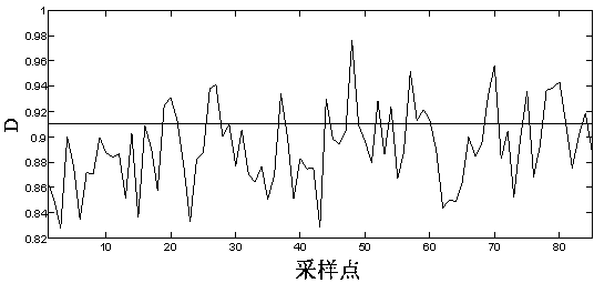
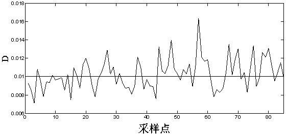
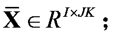
[0011] The invention aims at the monitoring problem of the semiconductor process, and first collects the normal historical data of the process by using the distributed control system. Then, the three-dimensional process data is expanded into an I×JK two-dimensional data matrix along the batch direction, preprocessed and normalized, and each data matrix is ​​rearranged along the time point direction to obtain a new data matrix. For the new two-dimensional data matrix, random sampling is carried out in the sample direction to obtain multiple two-dimensional independent data matrices, and for each two-dimensional independent data matrix, a support vector data description model is established to determine the super The center position and radius of the sphere. The modeling data and various model parameters are stored in the historical database and the real-time database for backup. When monitoring a new batch of data, different support vector data description models are used to m...


PUM


Abstract

The invention discloses a semiconductor process monitoring method based on the integrated leaning modeling technology. According to the semiconductor process monitoring method, on the basis that the vector data description algorithm is allowed, the integrated leaning modeling technology is introduced, and monitoring performance in a semiconductor process is promoted due to the fact that results of different models allowing vector data description are integrated. In an integrated leaning modeling process, a very important part is selection of appropriate integration strategies. As for the semiconductor process monitoring method, the different models allowing vector data description are integrated by adopting the advanced Bayesian reasoning strategy, and the advantages of all the models are used effectively. Finally, the semiconductor process is monitored by building a global statistic. Compared with a monitoring method based on a single model, the semiconductor process monitoring method based on the integrated leaning modeling technology greatly promotes the modeling performance of the models allowing vector data description and effectively improves the monitoring effect in the semiconductor process.

Description

technical field [0001] The invention belongs to the field of semiconductor industry process monitoring, in particular to a process monitoring method based on integrated learning modeling technology and support vector data description. Background technique [0002] Since the beginning of the 21st century, the monitoring of the production process of the semiconductor industry has attracted more and more attention from the industry and academia. This is because the process of the semiconductor industry itself has extremely high requirements on product quality. How to effectively prevent the process from producing inferior and unqualified products? The product is an urgent need to solve the problem. In addition, effective monitoring of the semiconductor process, the results obtained can in turn guide the improvement of the production process and production process. In addition to the method based on the mechanism model, the traditional semiconductor process monitoring methods m...

Claims


Application Information

Patent Timeline
IPC IPC(8): G05B19/418
Inventor 葛志强宋执环
Owner ZHEJIANG UNIV
Learn More