Multilayer circuit board and manufacturing method thereof

A technology of multilayer circuit board and manufacturing method, which is applied in the direction of multilayer circuit manufacturing, printed circuit components, etc., and can solve problems affecting the accuracy and quality of circuit boards, low precision of manual slotting, and many human resources.

Active Publication Date: 2013-10-30
AVARY HLDG (SHENZHEN) CO LTD +1
View PDF4 Cites 11 Cited by
  • Summary
  • Abstract
  • Description
  • Claims
  • Application Information

AI Technical Summary

Problems solved by technology

During production, it is necessary to make a multi-layer circuit board first, and then use the method of manual slotting to dig out the grooves. The manual slotting method not only requires more human resources, but also the accuracy of manual slotting is not high, which will affect Board precision and quality

Method used


Image

  • Multilayer circuit board and manufacturing method thereof
  • Multilayer circuit board and manufacturing method thereof
  • Multilayer circuit board and manufacturing method thereof

Examples


Embodiment Construction

[0030] The multilayer circuit board provided by the technical solution and its manufacturing method will be further described in detail below in conjunction with the drawings and multiple embodiments.

[0031] The method for manufacturing a multilayer circuit board provided by the first embodiment of the technical solution includes steps:

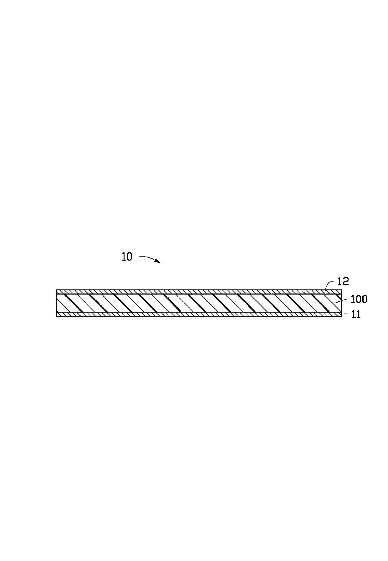
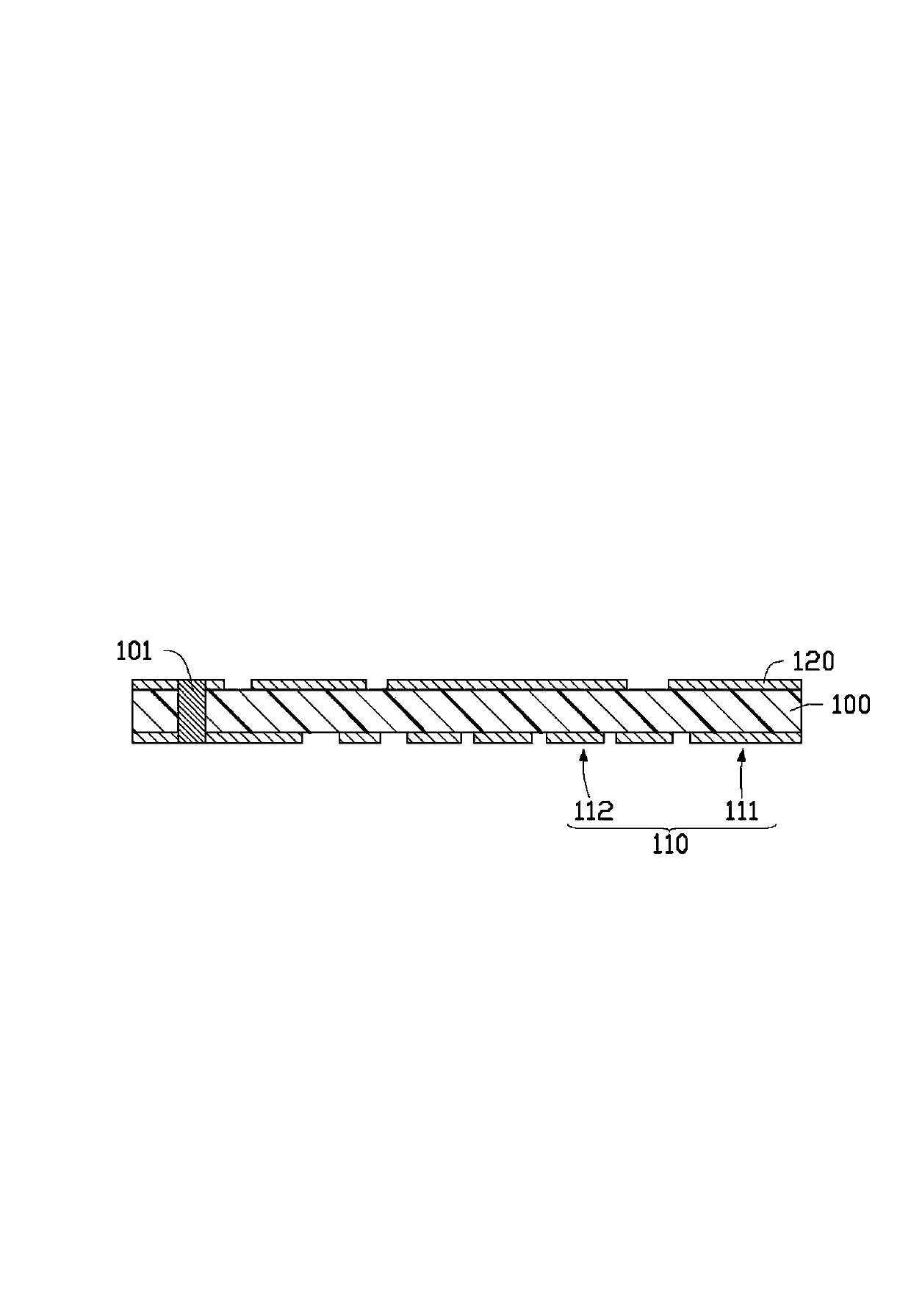
[0032] For a first step, see figure 1 , providing a circuit substrate 10 . In this embodiment, the circuit substrate 10 is a double-sided copper-clad laminate, including a first copper foil layer 11 , a base 100 and a second copper foil layer 12 laminated sequentially from bottom to top. The base 100 is an insulating layer made of insulating material. In other embodiments, the substrate 100 may be a multilayer substrate, that is, the substrate 100 may be a structure including multiple layers of copper foil layers and insulating layers arranged alternately. In other embodiments, the circuit substrate 10 may be a single-sided copper clad l...


PUM


Abstract

The invention provides a manufacturing method of a multilayer circuit board. The manufacturing method includes: (1) providing a circuit substrate, wherein the circuit substrate comprises a substrate body and a first copper foil layer attached to the surface of the substrate body, (2) manufacturing the first copper foil layer into a first conductive line layer, wherein the first conductive line layer is provided with a first exposed zone and a first pressing zone, (3) setting a first solder mask layer in the first exposed zone, (4) pressing a first alkali developable resin layer and a third copper foil layer on one side of the first conductive line layer of the circuit substrate, (5) forming a first opening corresponding to the first exposed zone in the third copper foil layer so as to expose the first alkali developable resin layer corresponding to the first exposed zone, (6) exposing the first alkali developable resin layer exposed out of the first opening, and (7) dissolving the exposed first alkali developable resin layer through an alkali developing solution so as to form a groove, wherein the first solder mask layer is exposed in the groove. The invention further provides the multilayer circuit board manufactured by means of the manufacturing method.

Description

technical field [0001] The invention relates to circuit board technology, in particular to a multilayer circuit board with grooves and a manufacturing method thereof. Background technique [0002] In the information, communication and consumer electronics industries, circuit boards are an indispensable and basic component of all electronic products. With the development of electronic products in the direction of miniaturization and high speed, circuit boards are also developing from single-sided circuit boards to double-sided circuit boards and multi-layer circuit boards. Multilayer circuit boards, especially embedded multilayer circuit boards with embedded electronic components, are widely used. Please refer to Takahashi, A. and others published in IEEE Trans. on Components, Packaging, and Manufacturing in 1992 Technology's literature "High density multilayer printed circuit board for HITAC M~880". [0003] Embedded circuit boards generally have a groove for embedding ele...

Claims


Application Information

Patent Timeline
Patent Type & Authority Applications(China)
IPC IPC(8): H05K3/46H05K1/02
Inventor 李清春
Owner AVARY HLDG (SHENZHEN) CO LTD
Why Eureka
Try Eureka