

Split gate resistor structure and manufacturing method thereof
A manufacturing method and resistor technology, which are applied in the direction of electric solid device, semiconductor/solid state device manufacturing, circuits, etc., can solve the problems of inability to change the width of the split gate resistor 20, poor practicability and flexibility, etc., and improve practicability. and the effect of flexibility
- Summary
- Abstract
- Description
- Claims
- Application Information
AI Technical Summary
Problems solved by technology
Method used
Image

Examples
Embodiment Construction
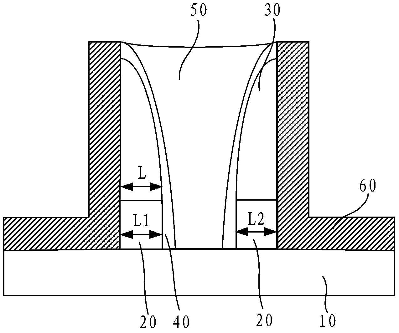
[0040] The split-gate resistor structure and its manufacturing method proposed by the present invention will be further described in detail below with reference to the accompanying drawings and specific embodiments. Advantages and features of the present invention will be apparent from the following description and claims. It should be noted that all the drawings are in a very simplified form and use imprecise scales, and are only used to facilitate and clearly assist the purpose of illustrating the embodiments of the present invention.
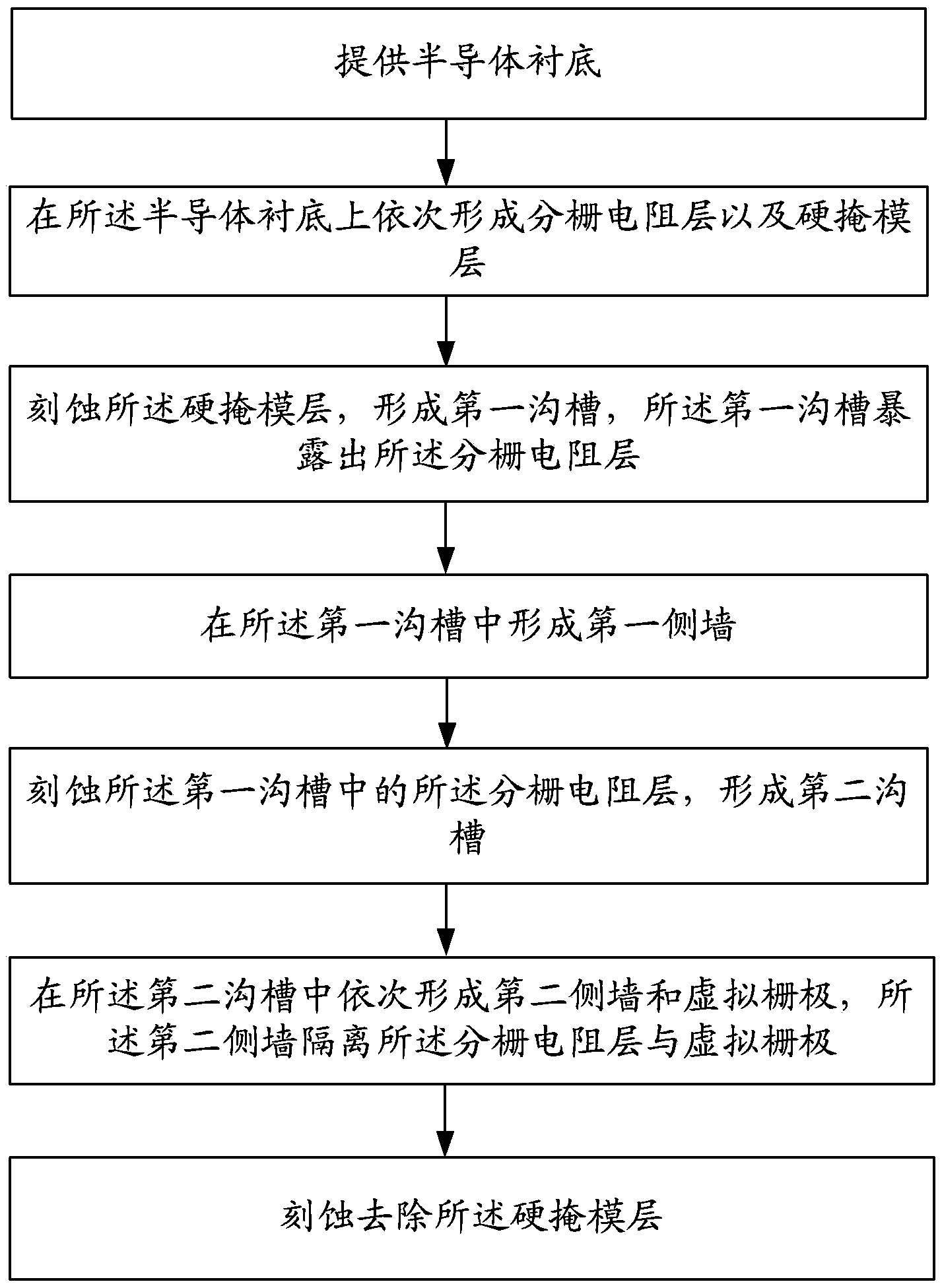
[0041] Please refer to figure 2 , the present embodiment proposes a method for fabricating a split-gate resistor, comprising the steps of:
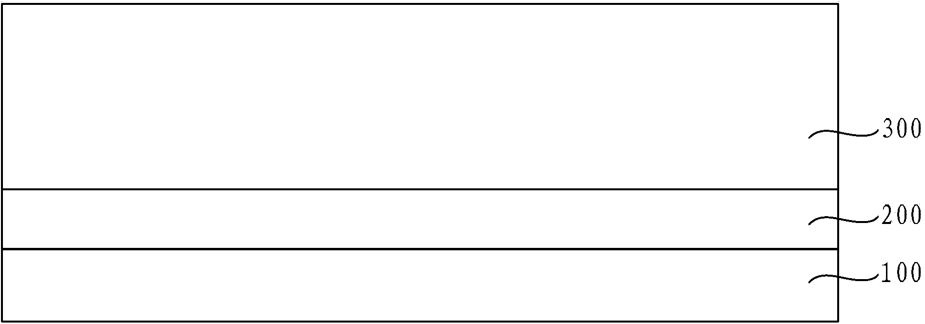
[0042] First, a semiconductor substrate is provided, and the semiconductor substrate is provided with a shallow trench isolation layer 100;
[0043] Next, the divided gate resistance layer 200 and the hard mask layer 300 are sequentially formed on the shallow trench isolation layer 100 of the semicond...
PUM
| Property | Measurement | Unit |
|---|---|---|
| Thickness | aaaaa | aaaaa |
| Thickness | aaaaa | aaaaa |
| Width | aaaaa | aaaaa |
Abstract
Description
Claims
Application Information