

Pixel structure of CMOS image senor and forming method thereof
An image sensor and pixel structure technology, applied in the field of image sensors, can solve problems such as affecting image quality, and achieve the effects of improving image quality, high image quality, and reducing afterimages.
- Summary
- Abstract
- Description
- Claims
- Application Information
AI Technical Summary
Problems solved by technology
Method used
Image

Examples
Embodiment Construction
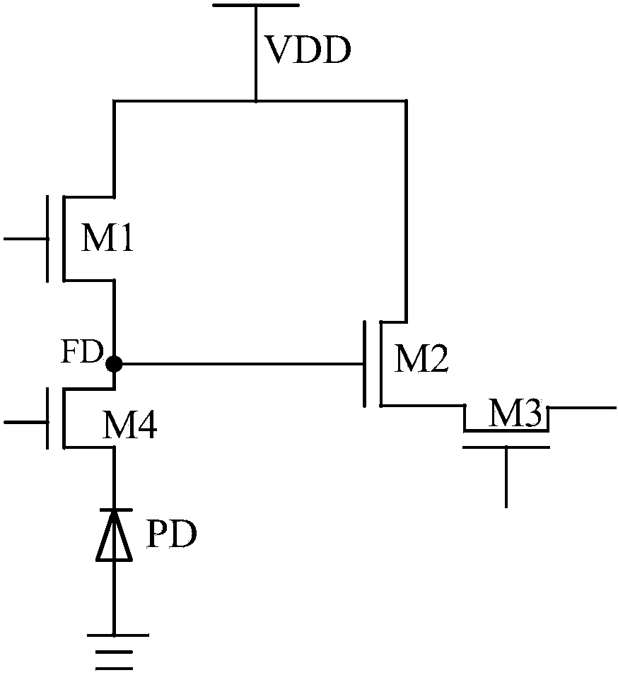
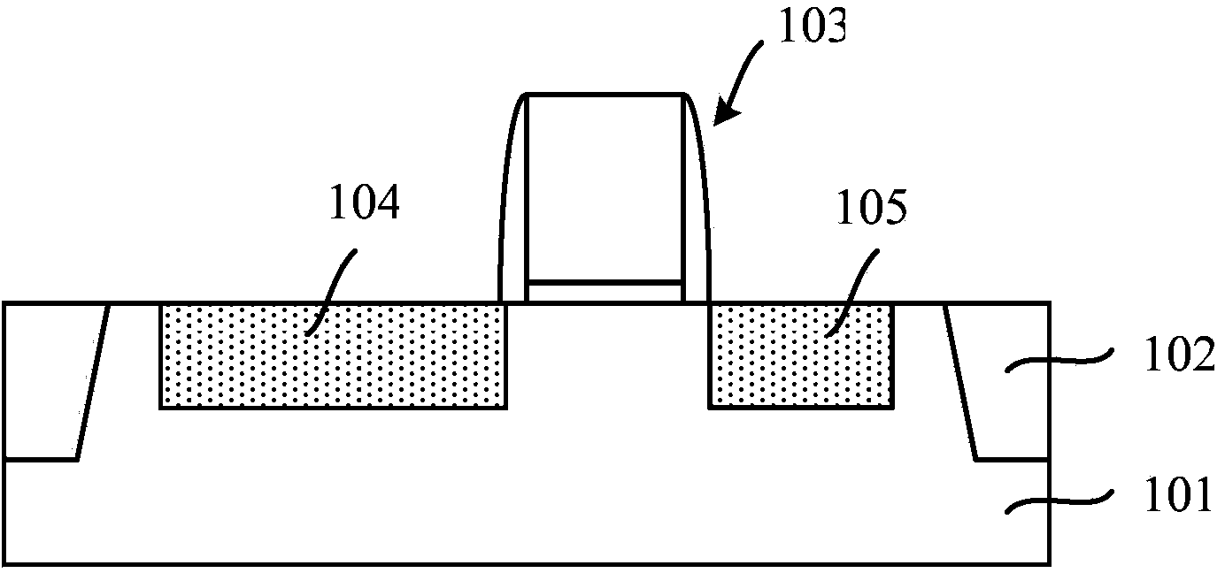
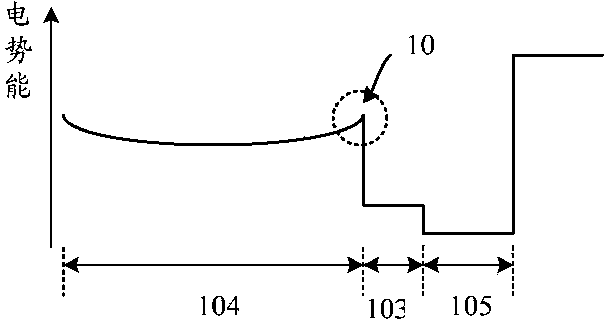
[0036] For the existing N-type CMOS image sensor pixel structure, please refer to figure 2 , the CMOS image sensor pixel structure includes: a P-type semiconductor substrate 101, a transfer transistor 103 located on the P-type semiconductor substrate 101, and the transfer transistor 103 includes a gate structure located on the P-type semiconductor substrate 101; A photodiode in the P-type semiconductor substrate on one side of the gate structure, the photodiode includes an N-type deeply doped region 104 located in the P-type semiconductor substrate, and the N-type deeply doped region 104 serves as the P-type of the photodiode The semiconductor substrate 101 serves as the anode of the photodiode; the N-type floating diffusion region 105 is located in the other side of the P-type semiconductor substrate 101 .
[0037] The formation process of the N-type deeply doped region 104 of the photodiode is as follows: firstly, a mask layer is formed on the P-type semiconductor substrate...
PUM
 Abstract
Description
Claims
Application Information