Substrate, light-emitting device, and illumination device

A technology for substrates and light-emitting elements, which is applied in the field of light-emitting devices, lighting devices, and substrates. It can solve problems such as low resistance, increased wiring resistance, and difficult metal wiring thickness, and achieve the effect of achieving insulation distance and suppressing voltage rise.

Inactive Publication Date: 2014-09-10
PANASONIC CORP
View PDF5 Cites 0 Cited by
  • Summary
  • Abstract
  • Description
  • Claims
  • Application Information

AI Technical Summary

Problems solved by technology

[0013] Furthermore, as the substrate becomes thinner, the metal wiring becomes thinner and thinner, and as the material of the metal wiring, instead of using low-resistance copper, silver with a relatively high resistance value is often used. Therefore, even if it is the same as conventional The width of the metal wiring also tends to increase the wiring resistance
In addition, metal wiring is often formed by printing, so it is also difficult to increase the thickness of the metal wiring to achieve low resistance.

Method used


Image

  • Substrate, light-emitting device, and illumination device
  • Substrate, light-emitting device, and illumination device
  • Substrate, light-emitting device, and illumination device

Examples


Embodiment 1

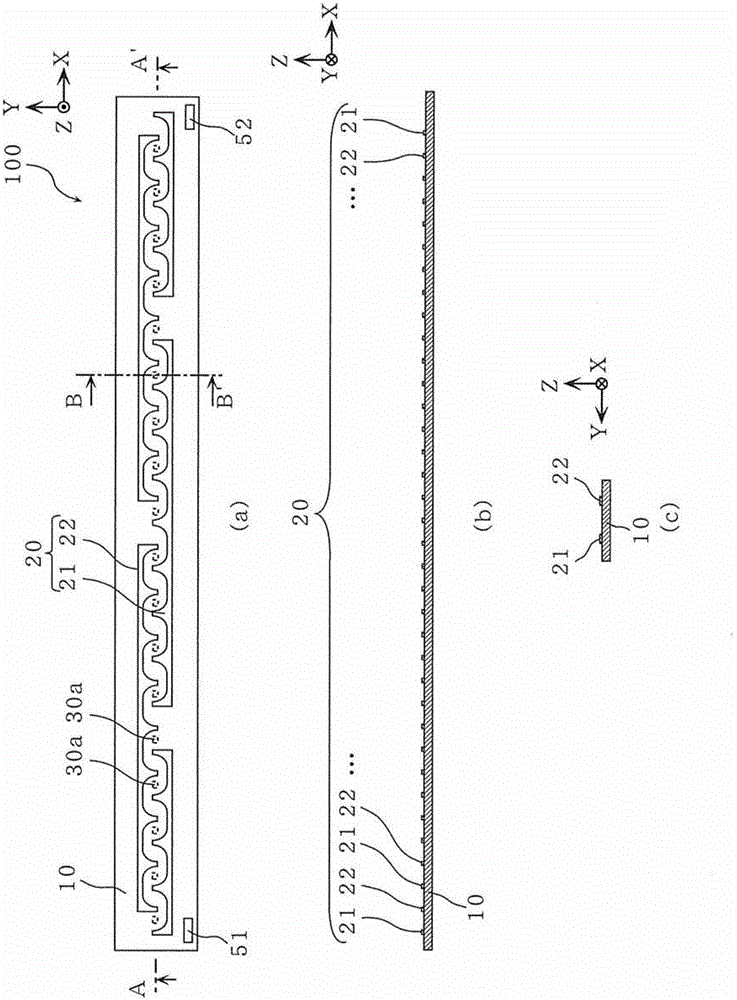
[0061] First, use figure 1 The configuration of the mounting substrate 100 according to the first embodiment of the present invention will be described. figure 1 (a) is a plan view of the mounting substrate according to Embodiment 1 of the present invention, figure 1 (b) is a cross-sectional view of the mounting substrate cut along the line AA' of (a) (substrate longitudinal cross-section), figure 1 (c) is a cross-sectional view (substrate short-direction cross-section) of the mounting substrate cut along line BB' of (a). Furthermore, the long direction of the substrate 10 is defined as the X-axis direction, the short direction of the substrate 10 as the direction perpendicular to the X-axis is defined as the Y-axis direction, and the direction perpendicular to the X-axis and the Y-axis is defined as a direction relative to The direction perpendicular to the principal surface of the substrate 10 is referred to as the Z-axis direction.

[0062] Such as figure 1 (a) to (c) s...

Embodiment 2

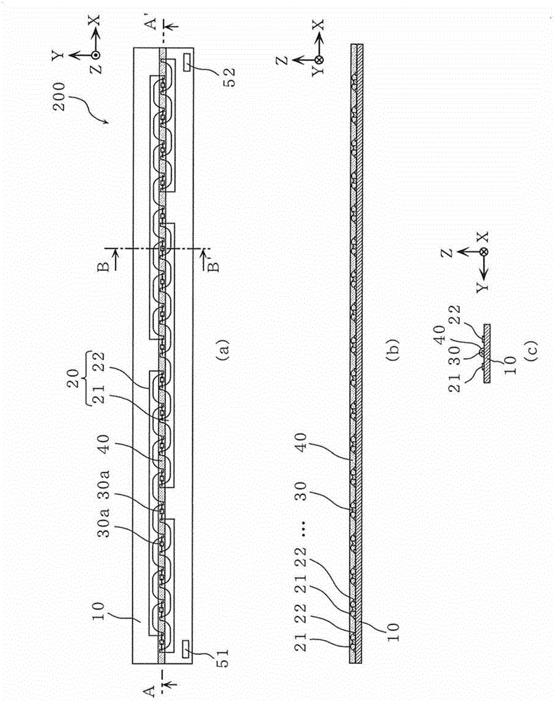
[0120] Next, use Figure 5 A mounting substrate 100X and a light emitting device according to Embodiment 2 of the present invention will be described. Figure 5 It is a partially enlarged view of a mounting substrate according to Embodiment 2 of the present invention.

[0121] Since the mounting substrate 100X and the light emitting device according to this embodiment have the same basic structure as the mounting substrate 100 and the light emitting device 200 according to the first embodiment, the following description will focus on the differences between the two. In addition, the same reference numerals are assigned to the same components of the present embodiment as in the first embodiment, and detailed descriptions are omitted or simplified. Furthermore, in the light-emitting device of this embodiment, using Figure 5 The mounting substrate 100X is shown.

[0122] In the mounting substrate 100X and the light-emitting device according to this embodiment, as in the first...

Embodiment 3

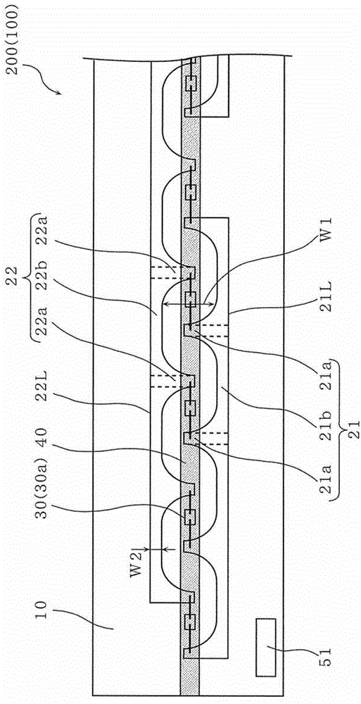
[0136] Next, use Image 6 A mounting substrate 100Y and a light emitting device 200Y according to Embodiment 3 of the present invention will be described. Image 6 (a) is a partially enlarged view of a mounting substrate according to Embodiment 3 of the present invention, Image 6 (b) is a partially enlarged view of a light emitting device according to Example 3 of the present invention.

[0137] Since the mounting substrate 100Y and the light emitting device 200Y according to the present embodiment have the same basic structure as the mounting substrate 100 and the light emitting device 200 according to the first embodiment, the following description will focus on their differences. In addition, the same reference numerals are assigned to the same components of the present embodiment as in the first embodiment, and detailed descriptions are omitted or simplified.

[0138] exist figure 1 In the mounting substrate 100 of the shown embodiment 1, the LED mounting positions 30a...


PUM


Abstract

A substrate (10) on which LEDs (30) are to be mounted to form an element row and which includes a first line (21) and a second line (22) disposed such that the element row is interposed therebetween. The first line (21) includes a first main line portion (21b) extending mainly in the row direction of the element row, and a first connecting portion (21a) connected to the first main line portion (21b) and including a portion for connecting to the LEDs (30). The second line (22) includes a second main line portion (22b) extending mainly in the row direction of the element row, and a second connecting portion (22a) connected to the second main line portion (22b) and including a portion for connecting to the LEDs (30). The gap between the first main line portion (21b) and the second main line portion (22b) is larger at LED mounting positions (30a) than at positions other than the LED mounting positions (30a).

Description

technical field [0001] The present invention relates to a substrate, a light-emitting device, and a lighting device, and particularly relates to a substrate on which a semiconductor light-emitting element is mounted, a light-emitting device using the semiconductor light-emitting element, and a lighting device using the semiconductor light-emitting element. Background technique [0002] In recent years, semiconductor light-emitting elements such as light-emitting diodes (LED: Light Emitting Diode) have been widely used in various devices as high-efficiency and space-saving light sources, for example, as backlight sources in liquid crystal display devices, or as It is used as a light source for lighting in lighting devices such as basic lighting and straight tube LED lamps. In this case, LEDs are unitized into LED modules and incorporated in various devices. [0003] As such an LED module, for example, Patent Document 1 discloses a COB (Chip On Board: Chip On Board) type ligh...

Claims


Application Information

Patent Timeline
Patent Type & Authority Patents(China)
IPC IPC(8): H01L33/62F21S2/00F21V23/00F21Y101/02
CPCH01L25/0753H01L2924/0002H05K1/181H01L33/62H01L27/153H01L2924/00
Inventor 杉浦健二阿部益巳
Owner PANASONIC CORP
Why Eureka
Try Eureka