Method of Shrinking Critical Dimensions in Dry Etching of Polysilicon Gate

A critical dimension and dry etching technology, which is applied in the direction of electrical components, semiconductor/solid-state device manufacturing, circuits, etc., can solve problems such as impact on subsequent processes, PR collapse, wafer surface defects, etc., and achieve enhanced etching resistance , control the degree of shrinkage, and meet the effect of process requirements

Active Publication Date: 2016-03-23
SHANGHAI HUALI MICROELECTRONICS CORP
View PDF4 Cites 0 Cited by
  • Summary
  • Abstract
  • Description
  • Claims
  • Application Information

AI Technical Summary

Problems solved by technology

This plasma reduction step can be carried out for photoresist (PR: photoresist). PRtrimming will etch the bottom anti-reflective coating (BARC: Bottom Anti-Reflective Coating) at the same time, and more PR can be left, but after PRtrimming, PR The aspect ratio will become larger, prone to PR collapse
It can also be carried out after BARC etching. The problem with this process method is the special process parameter setting of the process step of plasma reduction. This setting is an etching step that tends to be isotropic, and it is easy to be etched on the surface of the wafer. Defects are generated. In order to reduce the etching of the underlying material and increase the reduction on both sides of PR and BARC, this process step uses halogen-containing gas (fluorine, chlorine or hydrogen bromide) plus oxygen, and RF bias energy (RFbiaspower) If it is zero, the polymer attached to the side wall of the reaction chamber will be bombarded and dropped by oxygen-rich ions, causing defects on the wafer surface, and the plasma bombardment will also deteriorate the line width roughness (LWR) of the pattern
The third method is carried out after the hardmask etching is completed, but the trimming rate is relatively slow, which affects the production capacity
However, the method of this invention cannot control the degree of shrinkage of the key dimensions of the photoresist pattern, and the shrinkage may be insufficient or transitional, which will have an impact on the subsequent process, and there are also potential process problems

Method used


Image

  • Method of Shrinking Critical Dimensions in Dry Etching of Polysilicon Gate
  • Method of Shrinking Critical Dimensions in Dry Etching of Polysilicon Gate
  • Method of Shrinking Critical Dimensions in Dry Etching of Polysilicon Gate

Examples


Embodiment Construction

[0024] The present invention will be further described below in conjunction with the accompanying drawings and specific embodiments, but not as a limitation of the present invention.

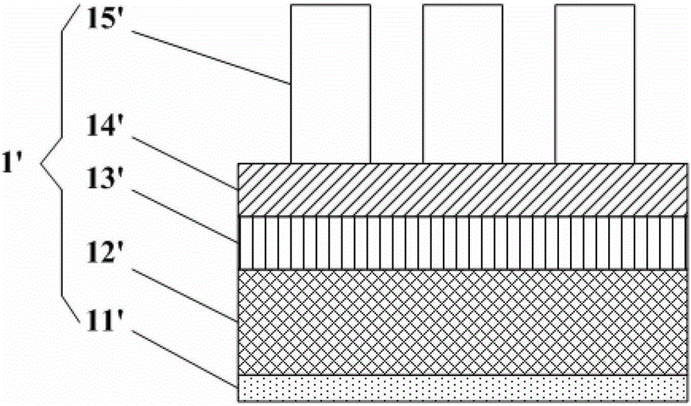
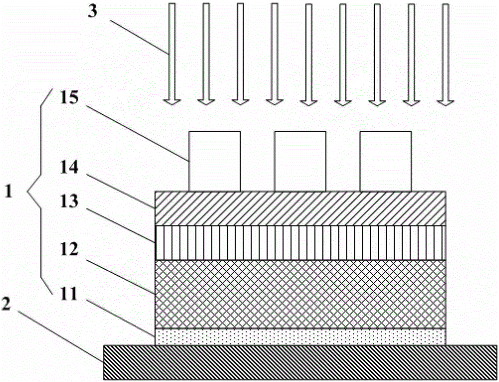
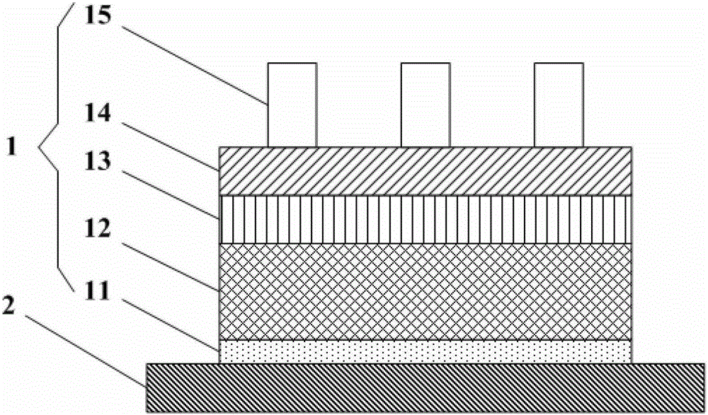
[0025] As an embodiment of the present invention, this embodiment relates to a method for shrinking critical dimensions in polysilicon gate dry etching, which includes the following steps: placing the exposed and developed wafer on the bottom plate of a back-baking device; At the same time, carry out back-baking and electron beam bombardment on the above-mentioned exposed and developed wafers, and control the photoresist shrinkage rate according to the process requirements; after the photoresist shrinkage rate meets the process requirements, stop the back-baking and electron beam bombardment of the above-mentioned exposed and developed wafers Electron beam bombardment: cooling the wafer after the exposure and development of the above stop back baking and electron beam bombardment to normal temper...


PUM


Abstract

The invention discloses a method for shrinking a critical size in polysilicon gate dry etching. The method includes the following steps that an exposed and developed silicon wafer is placed on a base pate of a back drying device; meanwhile, back drying and electron beam bombardment are simultaneously performed on the exposed and developed silicon wafer, and a light resistance shrinking percentage is controlled according to technological needs; after the light resistance shrinking percentage meets the technological needs, the back drying and the electron beam bombardment performed on the exposed and developed silicon wafer are stopped; the exposed and developed silicon wafer is cooled to normal temperature after the back drying and the electron beam bombardment are stopped, and then latter technologies are carried out. The method has the advantages that through the method of the combination of electron beams and the back drying, light resistance can be rapidly shrunk, the degree of the light resistance shrinking can be effectively controlled, and the technological needs are met. Meanwhile, the anti-etching capacity of the light resistance is enhanced, the selection ratio of the etching is effectively improved, and the effect that the same etching purpose is achieved with thinned needed optical resist is achieved. Therefore, the optical resist is saved, and the waste of resources is reduced.

Description

technical field [0001] The invention relates to the technical field of semiconductor preparation, in particular to a method for shrinking key dimensions in polysilicon gate dry etching. Background technique [0002] Polysilicon gate etching is one of the key processes for the formation of CMOS devices in the production of integrated circuits. With the advancement of technology and the requirements of market development, the size of semiconductor devices is continuously shrinking, and the requirements for photolithography processes are also increasing. In lithography, two factors that play a key role in image quality are resolution (R=k*λ / NA) and depth of focus DOF=λ / 2(NA) 2 , the photolithography process should not only have good resolution to obtain graphics of key dimensions, but also maintain a suitable depth of focus. However, the photolithography process has a certain limit, which creates a dilemma that the continuous reduction of the patterned critical dimension will ...

Claims


Application Information

Patent Timeline
Patent Type & Authority Patents(China)
IPC IPC(8): H01L21/3105G03F7/40
Inventor 高慧慧杨渝书秦伟李程
Owner SHANGHAI HUALI MICROELECTRONICS CORP
Why Eureka
Try Eureka