Method for preparing SGOI or GOI by utilizing C adulteration SiGe preparing layer

A technology for modulating layer and doping concentration, which is applied in the field of semiconductor material preparation, and can solve problems such as defects, affecting SGOI or GOI performance, lattice mismatch, etc.

Active Publication Date: 2013-12-25
SHANGHAI INST OF MICROSYSTEM & INFORMATION TECH CHINESE ACAD OF SCI
View PDF3 Cites 1 Cited by
  • Summary
  • Abstract
  • Description
  • Claims
  • Application Information

AI Technical Summary

Problems solved by technology

However, in the process of making SGOI/GOI by the traditional Ge concentration process, due to the lattice mismatch between the SiGe/Si int

Method used


Image

  • Method for preparing SGOI or GOI by utilizing C adulteration SiGe preparing layer
  • Method for preparing SGOI or GOI by utilizing C adulteration SiGe preparing layer
  • Method for preparing SGOI or GOI by utilizing C adulteration SiGe preparing layer

Examples


Embodiment 1

[0040] Such as Figure 1 ~ Figure 6 As shown, this embodiment provides a method for preparing SGOI or GOI by using a C-doped SiGe modulation layer, which at least includes the steps:

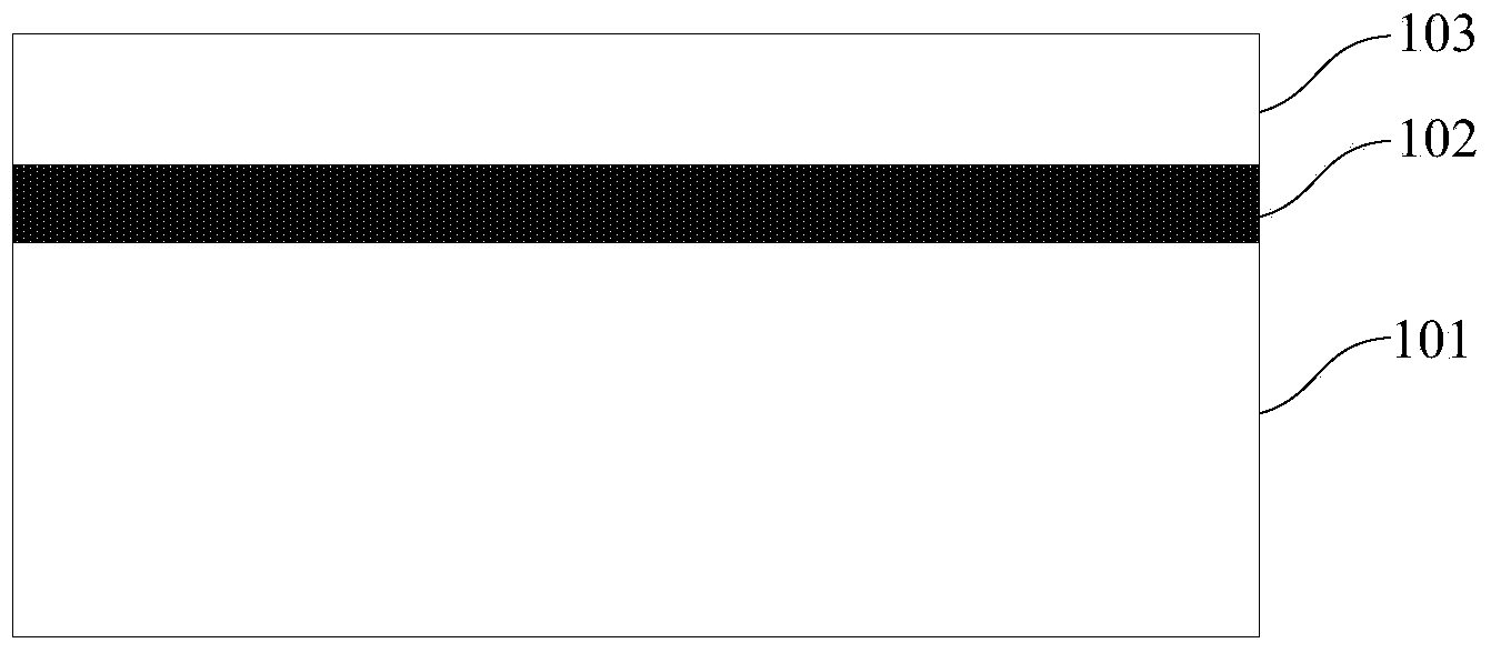
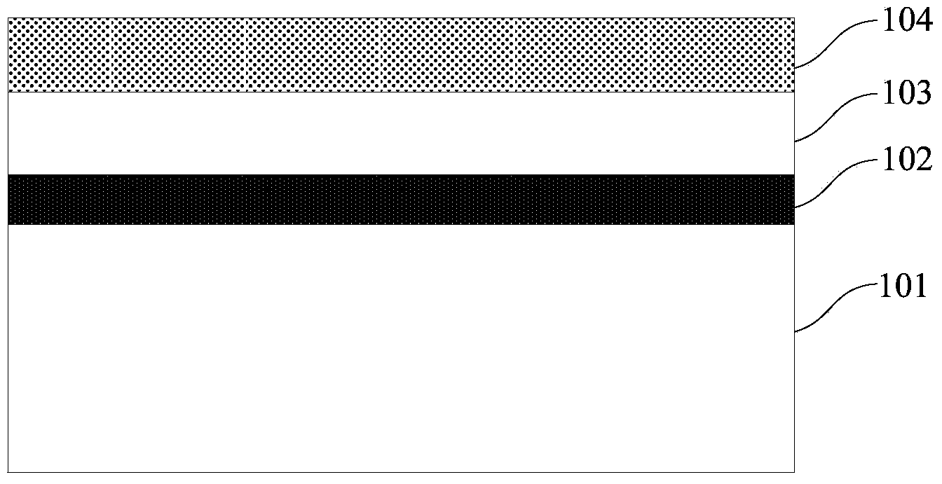
[0041] Such as Figure 1 ~ Figure 2 As shown, step 1) is first performed to provide an SOI substrate including a silicon substrate 101, a buried oxide layer 102 and a top silicon layer 103, and a C-doped SiGe modulation layer 104 is formed on the surface of the top silicon layer 103.

[0042] As an example, in the C-doped SiGe modulation layer 104, the doping concentration of C is not less than 1E20 / cm 3 . In this embodiment, in the C-doped SiGe modulation layer 104, the doping concentration of C is a constant value. Specifically, in the C-doped SiGe modulation layer 104, the doping concentration of C is 3E20 / cm 3 .

[0043] As an example, the thickness of the C-doped SiGe modulation layer 104 is not less than 20 nm and not greater than its critical thickness. In this embodiment, the thickness of the...

Embodiment 2

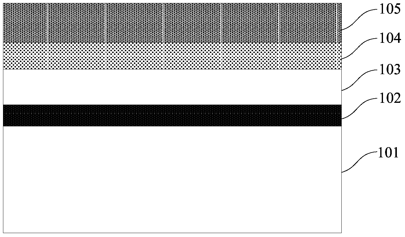
[0056] Such as Figure 1 ~ Figure 6 As shown, this embodiment provides a method for preparing SGOI or GOI using a C-doped SiGe modulation layer. The basic steps are the same as those in Embodiment 1. In the C-doped SiGe modulation layer 104, the doping concentration of C is not Instead, it gradually decreases from bottom to top, that is, the C concentration near the top silicon layer 103 is high, and the C concentration near the SiGe material layer 105 is low, so that the top silicon layer 103 of SOI and the epitaxial SiGe material can be better adjusted The lattice mismatch between the layers 105 reduces the occurrence of defects.

[0057] As described above, the present invention provides a method for preparing SGOI or GOI using a C-doped SiGe modulation layer, which includes the steps: 1) Provide an SOI substrate including a silicon substrate, a buried oxide layer and a top silicon layer, and A C-doped SiGe modulation layer is formed on the surface of the silicon layer; 2) a ...


PUM

PropertyMeasurementUnit
Thicknessaaaaaaaaaa
Thicknessaaaaaaaaaa
Thicknessaaaaaaaaaa

Abstract

The invention provides a method for preparing SGOI or GOI by utilizing a C adulteration SiGe preparing layer. The method comprises the first step of forming the C adulteration SiGe preparing layer on the surface of a top silicon layer of SOI, the second step of forming an SiGe material layer on the surface of the C adulteration SiGe preparing layer, the third step of forming an Si cap layer on the surface of the SiGe material layer, the fourth step of oxidizing annealing the structure to oxidize the Si cap layer and gradually oxidize the SiGe material layer, the C adulteration SiGe preparing layer and the top silicon layer to enable Ge in the SiGe material layer and the C adulteration SiGe preparing layer be diffused to the top silicon layer and gradually concentrated and forming a top SiGe layer or a top Ge layer and an SiO2 layer on the upward side, and the fifth step of removing the SiO2 layer. Lattice mismatch between the SOI top silicon layer and the epitaxial SiGe material layer is reduced through the C adulteration SiGe preparing layer, and accordingly defects produced in the process of concentration are reduced. The prepared SGOI has the advantages of being high in relaxation, low in defect density, high in Ge component and the like.

Description

Technical field [0001] The invention relates to a method for preparing semiconductor materials, in particular to a method for preparing SGOI or GOI by using a C-doped SiGe modulation layer. Background technique [0002] With the rapid development of silicon-based large-scale integrated circuit technology, the performance of bulk silicon CMOS devices has gradually approached the physical limit of silicon materials. Further improving the performance of bulk silicon CMOS devices along the direction of Moore's law will face increasing investment And market risk. The semiconductor industry is a very sensitive market for product performance-price ratios. How to continuously improve the performance of silicon-based devices on the basis of the existing VLSL process without increasing investment has become a common problem in the industry. The exploration of new materials and new processes will undoubtedly become an important idea and research direction for solving this problem. [0003]...

Claims


Application Information

Patent Timeline
IPC IPC(8): H01L21/762
Inventor 张苗陈达狄增峰薛忠营叶林王刚母志强
Owner SHANGHAI INST OF MICROSYSTEM & INFORMATION TECH CHINESE ACAD OF SCI
Why Eureka
Try Eureka