A semiconductor feeding device with anti-warping function

A technology of semiconductor and pushing device, which is applied in semiconductor/solid-state device manufacturing, transportation and packaging, conveyor objects, etc., can solve the problems of easy deformation and damage of lead feet, reduced product integrity, low strength of plastic-encapsulated lead frames, etc. Easy to operate and maintain, prevent warping and deformation, and improve the effect of stability

Active Publication Date: 2016-05-25
TONGLING SANJIA YAMADA TECH
View PDF4 Cites 0 Cited by
  • Summary
  • Abstract
  • Description
  • Claims
  • Application Information

AI Technical Summary

Problems solved by technology

[0002] At present, the domestic integrated circuit IC manufacturing industry has higher and higher requirements for the qualified rate of products. The plastic-encapsulated lead frame after welding the gold wire pins and chips is taken out from the special material box by a special manipulator and put into the feeding track. The push rod is pushed to the limit block, and finally the plastic-encapsulated lead frame is gradually sent into the automatic punching and forming mold by the feeding claw according to the fixed value step, but the thinnest lead pin thickness is only 0.15mm , The thickest one is only 0.6mm, and the strength of the plastic-encapsulated lead frame is low. Therefore, if the push rod rigidly pushes the plastic-enclosed lead frame to the limit block, the lead pin is easily deformed and damaged when encountering resistance, which will reduce the integrity rate of the product

Method used


Image

  • A semiconductor feeding device with anti-warping function
  • A semiconductor feeding device with anti-warping function
  • A semiconductor feeding device with anti-warping function

Examples


Embodiment Construction

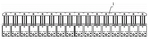
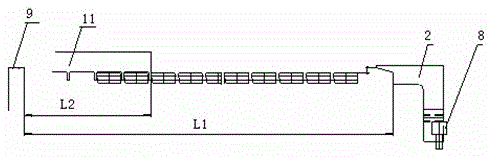
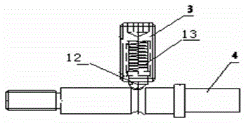
[0018] Such as figure 1 and figure 2 As shown, a semiconductor feeding device that can effectively prevent plastic lead frame 1 from warping and deforming during processing includes an open feeding track 10 and a pushing device, such as Figure 5 and Figure 6 As shown, the mold cavity of the feeding track 10 matches the shape of the pushed plastic-encapsulated lead frame 1, and there is a pushing device on the feeding track 10, such as Figure 4 , Figure 7 and Figure 8 As shown, the pushing device includes push rod 2, push rod connecting rod 4, push rod mounting block 6, sensor 5, roller follower 8 and transmission fixed plate 7, push rod mounting block 6, sensor 5 and roller follower The actuator 8 is fixed on the transmission fixed plate 7, the motor drives the transmission fixed plate 7, and then pushes the pushing device to reciprocate along the feeding track 10, and the push rod 2 is rigidly connected to the push rod connecting rod 4, such as image 3 As shown, t...


PUM


Abstract

The invention provides a semiconductor charging device capable of effectively preventing the buckling deformation of a plastic-packaged lead frame in a processing process. The semiconductor charging device comprises an open type charging track and a pushing device, wherein the cavity of the charging track is matched with the plastic-packaged lead frame; one end of the charging track is provided with a limited block; the pushing device comprises a push rod, a push rod installation block, a sensor, a roller, a follower and a conveying fixed plate; a push rod connecting rod is elastically connected with the push rod installation block through an elastic screw plug, controls elastic connecting force through the elastic screw plug and keeps effective connection under the condition that the plastic-packaged lead frame is not deformed and damaged; the slant hook-shaped design of the push rod is adapted to the buckling deformation of the plastic-packaged lead frame, wherein the deformation amount of the buckling deformation is less than h. The semiconductor charging device provided by the invention enhances the stability of equipment and the perfectness ratio of a product and is convenient to operate and maintain.

Description

technical field [0001] The invention relates to an automatic punching and forming equipment, in particular to a semiconductor feeding device with an anti-warping function. Background technique [0002] At present, the domestic integrated circuit IC manufacturing industry has higher and higher requirements for the qualified rate of products. The plastic-encapsulated lead frame after welding the gold wire pins and chips is taken out from the special material box by a special manipulator and put into the feeding track. The push rod is pushed to the limit block, and finally the plastic-encapsulated lead frame is gradually sent into the automatic punching and forming mold by the feeding claw according to the fixed value step, but the thinnest lead pin thickness is only 0.15mm , The thickest one is only 0.6mm, and the strength of the plastic-encapsulated lead frame is low. Therefore, if the push rod rigidly pushes the plastic-enclosed lead frame to the limit block, the lead pin is...

Claims


Application Information

Patent Timeline
Patent Type & Authority Patents(China)
IPC IPC(8): H01L21/56H01L21/677
Inventor 丁海生杨亚萍汪宗华郑翔
Owner TONGLING SANJIA YAMADA TECH
Why Eureka
Try Eureka