Compounds for electronic devices

A technology of compounds and atoms, applied in the field of compounds of formula, can solve the problems of limiting the life and efficiency of organic electroluminescence devices

Active Publication Date: 2014-01-08
MERCK PATENT GMBH
View PDF106 Cites 12 Cited by
  • Summary
  • Abstract
  • Description
  • Claims
  • Application Information

AI Technical Summary

Problems solved by technology

In particular, the properties of the host material often limit the lifetime and efficiency of organic electroluminescent devices

Method used


Image

  • Compounds for electronic devices
  • Compounds for electronic devices
  • Compounds for electronic devices

Examples


Embodiment 1

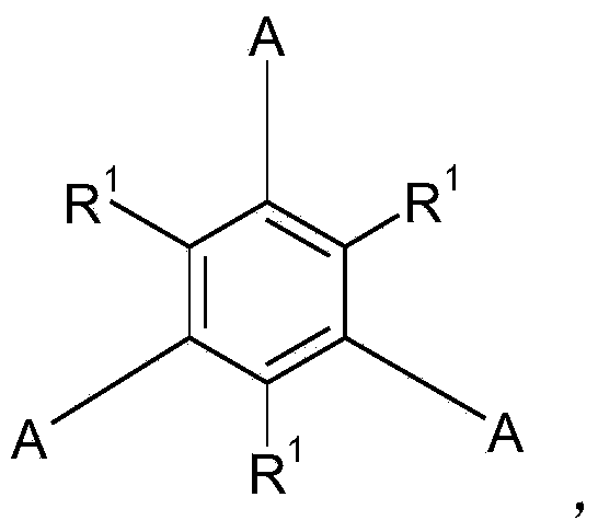
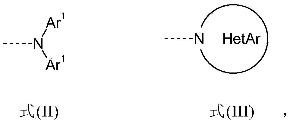
[0223] 2,4,6-Trimethyl-N,N,N',N',N'',N''-hexaphenylbenzene-1,3,5-triamine

[0224]

[0225] 14.0 ml (14 mmol) of 1M tri-tert-butylphosphine in toluene, 1.6 g (7 mmol) of palladium(II) acetate, and then 103.0 g (1.1 mol) of sodium tert-butoxide were added sequentially to 85.0 g (238 mmol) of 1 , 3,5-tribromo-2,4,6-trimethylbenzene [608-72-0] and 161.2g (953mmol) of diphenylamine in a solution of 2000ml of toluene. The reaction mixture was heated to reflux for 16 hours, allowed to cool to 60 °C, 20 ml of acetic acid and 250 ml of water were added, the mixture was allowed to cool to room temperature, the aqueous phase was separated, the organic phase was washed once with 500 ml of water and washed with 500 ml of saturated sodium chloride solution Wash once, then remove toluene under vacuum. The residue was washed by boiling once with 1000 ml of ethanol, dried in vacuo and then recrystallized six times from DMF (about 5 ml / g). Then in high vacuum (p about 10 -6 mbar, T about...


PUM

PropertyMeasurementUnit
thicknessaaaaaaaaaa

Abstract

The present invention relates to a compound of the formula (I), the use of this compound in an electronic device and also an electronic device containing one or more compounds of the formula (I). The invention further relates to the preparation of the compound of the formula (I) and also a formulation containing one or more compounds of the formula (I).

Description

technical field [0001] The present invention relates to compounds of formula (I), to the use of such compounds in electronic devices, and to electronic devices comprising one or more compounds of formula (I). The invention also relates to the preparation of compounds of formula (I) and to formulations comprising one or more compounds of formula (I). Background technique [0002] The development of new functional compounds for use in electronic devices is the subject of intense current research. The aim here is to develop and investigate compounds that have hitherto not been used in electronic devices and to develop compounds that can improve the profile of device properties. [0003] According to the present invention, the term electronic device is in particular taken to mean organic integrated circuits (OICs), organic field-effect transistors (OFETs), organic thin-film transistors (OTFTs), organic light-emitting transistors (OLETs), organic solar cells (OSCs), organic Opt...

Claims


Application Information

Patent Timeline
Patent Type & Authority Applications(China)
IPC IPC(8): C09K11/06H05B33/14H01L51/50H01L51/00
CPCC09K2211/185C09K2211/1033H01L51/0071H05B33/14C09K2211/1044H01L51/0061C09K2211/1037H01L51/0072H01L51/5048C09K2211/1007H01L51/0069C09K2211/1014H01L51/0059H01L51/5072H01L51/006H01L51/5016C09K11/06C09K2211/1059C09K2211/1029C09K2211/1011H01L51/5056Y02E10/549C09K2211/1022C07D209/86C07D235/18C07D249/18C07D265/38C09K11/025H10K85/633H10K85/631H10K85/6572H10K50/16H10K50/15H10K50/11H10K2101/10C07C211/43H10K50/00H10K85/657H10K85/656H10K50/18H10K85/626H10K2101/90C07C209/60C07C211/54C07C211/56C07C211/58C07C213/00C07C217/92C07C253/30C07C255/58C09K2211/1003C09K2211/1074
Inventor 菲利普·斯托塞尔阿尔内·比辛弗兰克·福格斯克里斯托夫·普夫卢姆埃米尔·侯赛因·帕勒姆托马斯·埃伯利特雷莎·穆希卡-费尔瑙德
Owner MERCK PATENT GMBH
Why Eureka
Try Eureka