Array substrate and preparing method thereof, display device and preparing method thereof

A technology for array substrates and display devices, applied in the fields of array substrates and their preparation, display devices and their preparations, can solve problems such as gate drive circuit damage, abnormal screen display, and failure to work normally, so as to improve reliability and avoid damage Effect

Inactive Publication Date: 2014-01-15
BEIJING BOE OPTOELECTRONCIS TECH CO LTD
View PDF6 Cites 46 Cited by
  • Summary
  • Abstract
  • Description
  • Claims
  • Application Information

AI Technical Summary

Problems solved by technology

[0008] However, although some liquid crystal display devices in the prior art have added and changed shapes and signals to prevent electrostatic breakdown, they are still prone to gate drive circuit damage caused by electrostatic breakdown under high-voltage test conditions above 2KV. , resulting in abnormal screen display, or even failure to work normally

Method used


Image

  • Array substrate and preparing method thereof, display device and preparing method thereof
  • Array substrate and preparing method thereof, display device and preparing method thereof
  • Array substrate and preparing method thereof, display device and preparing method thereof

Examples


Embodiment 1

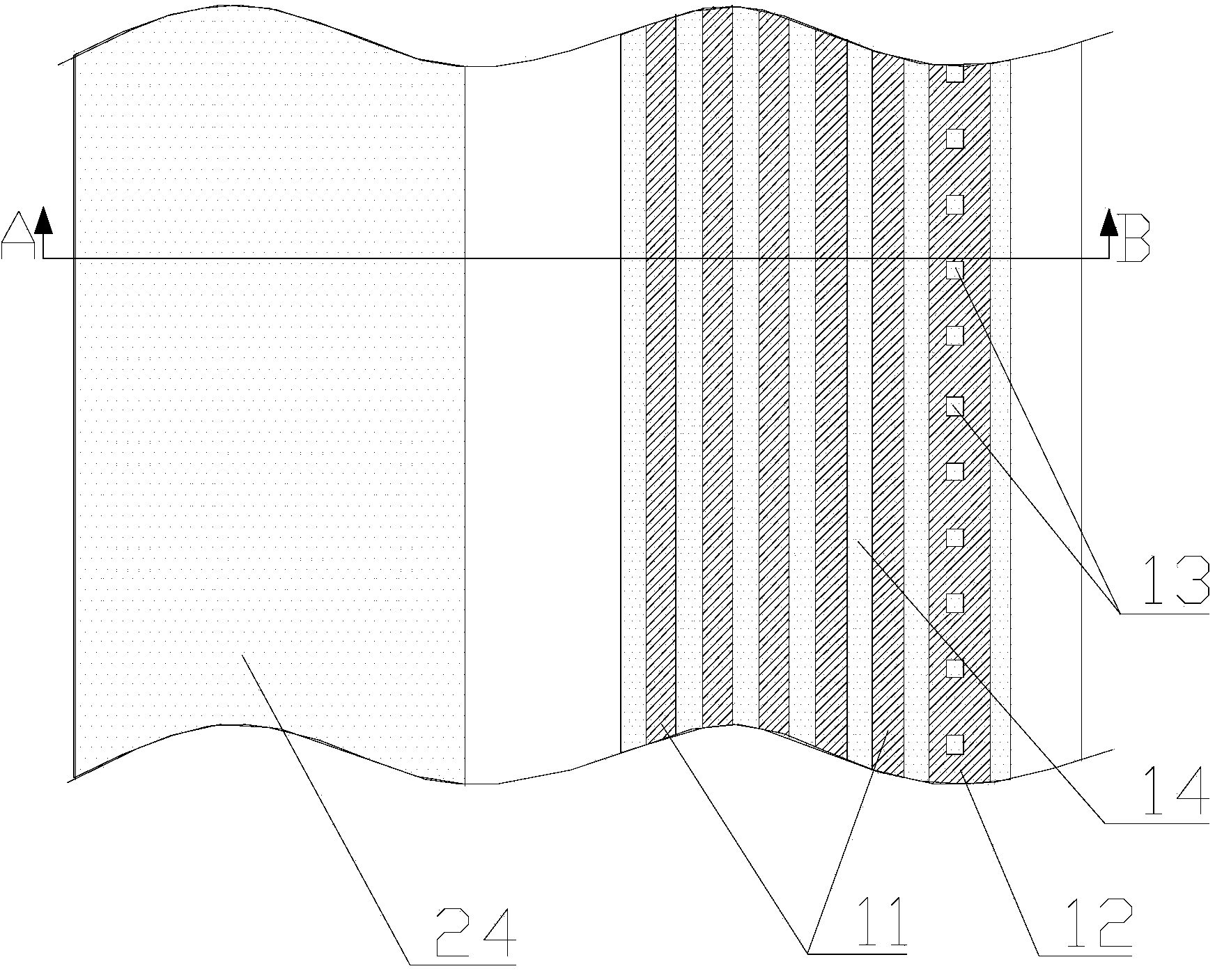
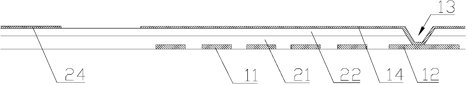
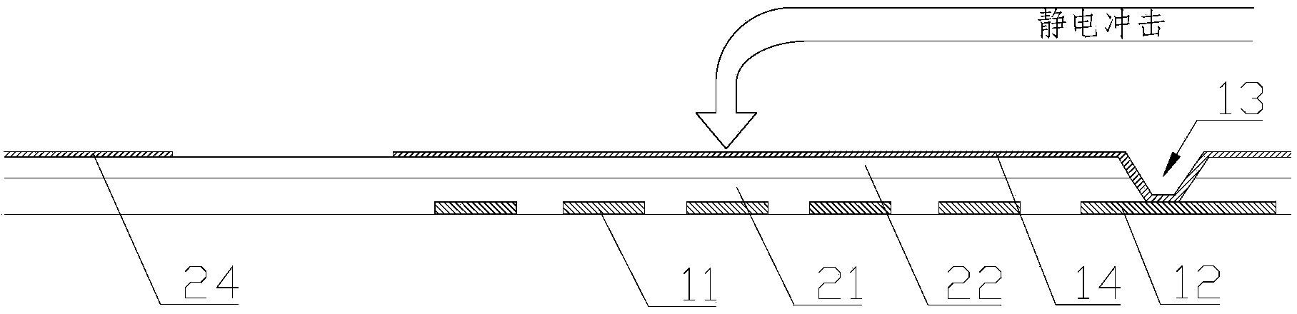
[0060] In this embodiment, the array substrate mainly includes a base substrate, which can be a glass substrate, a quartz substrate, or other flexible substrates, etc., and several pixel units are arranged on the base substrate, and each pixel unit usually includes a TFT, and the TFT Generally, it includes a source, a gate, and a drain. Each pixel unit may also include a pixel electrode, a common electrode, and a touch electrode. In addition, a touch electrode may also be provided on the array substrate. The TFT of each pixel unit needs to be connected with a corresponding driving circuit for providing driving signals for each TFT.

[0061] The above-mentioned drive circuits mainly include drive circuits such as gate drive circuits, source drive circuits, common electrode drive circuits, and touch drive circuits. Various drive circuits can be manufactured using the process of external chips, and can also be partially or completely arranged on the array substrate. Therefore, th...

Embodiment 2

[0070] The present invention also provides a display device using any one of the above-mentioned array substrates, the display device mainly comprising any one of the above-mentioned array substrates and a cell-aligning substrate disposed opposite to the array substrate.

[0071] The box-to-box substrate can be different depending on the type of display device; for example, in a liquid crystal display device, the box-to-box substrate can be a color filter substrate, while an OLED (Organic Light Emitting Diode, organic light-emitting diode) In a display device with a level tube), the pair of cell substrates may be a packaging substrate or the like.

[0072] Since the array substrate used in the display device is provided with a grounding structure including grounding leads and a first electrostatic protection layer, the grounding structure can be used to effectively protect the drive circuit provided on the array substrate from electrostatic shocks, thereby avoiding electrostati...


PUM


Abstract

The invention relates to the technical field of display, in particular to an array substrate, a preparing method of the array substrate, a display device with the array substrate and a preparing method of the display device. The array substrate comprises a substrate body. The substrate body is provided with a plurality of pixel units and a drive circuit used for driving the pixel units. The edge of the substrate body is further provided with a ground lead and a first electrostatic protection layer connected with the ground lead. According to the array substrate, the preparing method of the array substrate, the display device with the array substrate and the preparing method of the display device, the ground lead and the first electrostatic protection layer are arranged, so that when a static shock occurs, electrostatic charges are discharged through the ground lead and the first electrostatic protection layer, an effective static shock protection mechanism is formed, damage, caused by electrostatic breakdown, to the drive circuit is avoided, and the reliability of the product is greatly improved.

Description

technical field [0001] The present invention relates to the field of display technology, in particular to an array substrate and a preparation method thereof, a display device using the array substrate and a preparation method thereof. Background technique [0002] Compared with traditional cathode ray tube display devices, flat panel display devices have the advantages of thinness, low driving voltage, no flicker and jitter, and long service life. With the advantages of eliminating radiation, saving space, and saving energy, it is widely used in electronic products such as televisions, mobile phones, and display devices, and has occupied a dominant position in the field of flat-panel displays. [0003] The liquid crystal display device mainly includes a liquid crystal panel and a circuit system, etc. The liquid crystal panel includes an array substrate and a color filter substrate arranged oppositely. The array substrate is provided with a plurality of pixel units, and the ...

Claims


Application Information

Patent Timeline
Patent Type & Authority Applications(China)
IPC IPC(8): G02F1/133G02F1/1333
Inventor 姜文博陈小川王世君
Owner BEIJING BOE OPTOELECTRONCIS TECH CO LTD
Why Eureka
Try Eureka