A wide-illuminance full-color imaging detection chip

An illumination and full-color technology, applied in the field of imaging detection, can solve problems such as limited variable range, poor irradiation adaptability, and difficulty in extracting photoelectric signals, and achieve a large range of outgoing light intensity, good environmental adaptability, and high structural stability sexual effect

Active Publication Date: 2015-11-11
HUAZHONG UNIV OF SCI & TECH
View PDF5 Cites 0 Cited by
  • Summary
  • Abstract
  • Description
  • Claims
  • Application Information

AI Technical Summary

Problems solved by technology

The defects of this imaging system are mainly manifested in: (1) The fluctuation degree of the light intensity of the energy flow compression field constructed by the imaging optical system is restricted by the sensitivity threshold of the photosensitive material, and its variable range is relatively limited. The realization of low-speed mechanical operations such as the clear aperture of the imaging optical system cannot adapt to rapid changes in light intensity; (2) Photonic devices are limited by the distribution density of micro-nano photoelectric conversion structures, and their response to intensity changes in the irradiated light field The range is relatively narrow. If the light intensity is too high, it will be saturated. If the light intensity is too low, it will be difficult to extract the photoelectric signal due to the low signal-to-noise ratio or signal-to-clutter ratio. (4) Poor irradiation adaptability, unable to quickly adapt to drastic changes in the intensity of the incident light field; (5) Insufficient adaptability to the target and environment, unable to combine strong stray or interfering light with relatively weak target radiation , fused under a unified detection architecture

Method used


Image

  • A wide-illuminance full-color imaging detection chip
  • A wide-illuminance full-color imaging detection chip

Examples


Embodiment Construction

[0023] In order to make the object, technical solution and advantages of the present invention clearer, the present invention will be further described in detail below in conjunction with the accompanying drawings and embodiments. It should be understood that the specific embodiments described here are only used to explain the present invention, not to limit the present invention. In addition, the technical features involved in the various embodiments of the present invention described below can be combined with each other as long as they do not constitute a conflict with each other.

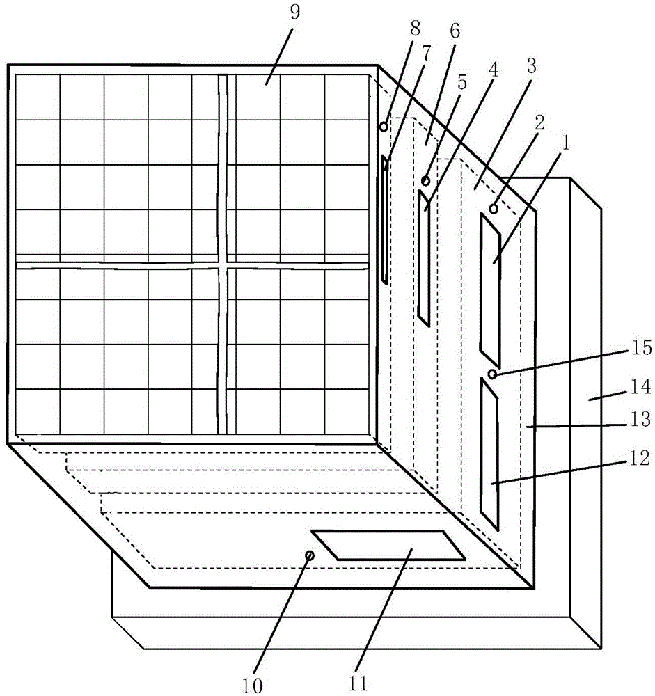
[0024] Such as figure 1 As shown, the wide-illuminance full-color imaging detection chip of the embodiment of the present invention includes: a ceramic shell 13, a metal support cooling plate 14, a drive control preprocessing module 3, an area array panchromatic detector 6, and an area array electronically controlled dual-mode planar liquid crystal microlens9.

[0025]The ceramic shell 13 is l...


PUM


Abstract

The invention discloses a wide-illuminance panchromatic imaging detection chip comprising an area array electronic-control dual-mode plane liquid crystal micro-lens, an area array panchromatic detector and a drive-control preprocessing module, wherein the area array panchromatic detector is divided into a plurality of array-distributed sub area array panchromatic detectors, each sub area array panchromatic detector comprises a plurality of array-distributed photosensitive elements with the same numbers and arrangement manners; the area array electronic-control dual-mode plane liquid crystal micro-lens is coupled with the area array panchromatic detector in a matching manner and comprises a plurality of array-distributed unit electronic-control dual-mode plane liquid crystal micro-lenses, and each unit electronic-control dual-mode plane liquid crystal micro-lens corresponds to one sub area array panchromatic detector; the area array electronic-control dual-mode plane liquid crystal micro-lens carries out oriented collection and dispersion on incident light or maintains the space transmission form of a light beam based on the intensity of the incident light. According to the wide-illuminance panchromatic imaging detection chip disclosed by the invention, the panchromatic image information in a wide illuminance range can be obtained, the measurement precision is high, the target and environment suitability is good, and the detection chip is easy to be coupled with a regular optical system.

Description

technical field [0001] The invention belongs to the technical field of imaging detection, and more specifically relates to a wide-illuminance full-color imaging detection chip. Background technique [0002] So far, panchromatic imaging devices based on the area-array focal plane photosensitive architecture have entered the family, and have become a basic means of image information acquisition in the fields of industrial and agricultural growth, teaching, scientific research, and national defense. For the core photosensitive array, whether it can continuously improve the ability to deal with strong light and low light targets in complex background environments has become an important source of power to promote the continuous and rapid development of arrayed photosensitive devices. So far, people have continuously developed photosensitive chips with larger and larger arrays, improved the photoelectric sensitivity of photosensitive materials, reduced photosensitive structural n...

Claims


Application Information

Patent Timeline
Patent Type & Authority Patents(China)
IPC IPC(8): G01J1/42G01J1/04
Inventor 张新宇康胜武佟庆罗俊张静赵慧桑红石谢长生
Owner HUAZHONG UNIV OF SCI & TECH
Why Eureka
Try Eureka