Testing device for determining compression creepage performance of microelectronic packing welding spots

A technology of microelectronic packaging and compression creep, which is applied in the direction of measuring devices, applying stable tension/pressure to test the strength of materials, and using optical devices, etc. Inconsistency between variable activation energy and stress index can achieve the effects of improving measurement accuracy, avoiding uneven distribution of compressive stress, and avoiding bias

Active Publication Date: 2014-01-22
DALIAN UNIV OF TECH
View PDF8 Cites 11 Cited by
  • Summary
  • Abstract
  • Description
  • Claims
  • Application Information

AI Technical Summary

Problems solved by technology

In particular, it is pointed out that the geometric particularity of the BGA package structure makes it easy to generate stress concentration in the solder joints located on the edge during service, and the stress state of the solder joints during service and the stress state in the bulk solder creep test also exist. The creep test results are not directly comparable, which makes the eigenvalues ​​representing the creep mechanism obtained in the relevant creep research: the creep activation energy and the stress index are not consistent, and the dispersion is large

Method used


Image

  • Testing device for determining compression creepage performance of microelectronic packing welding spots
  • Testing device for determining compression creepage performance of microelectronic packing welding spots
  • Testing device for determining compression creepage performance of microelectronic packing welding spots

Examples


Embodiment Construction

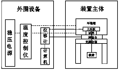
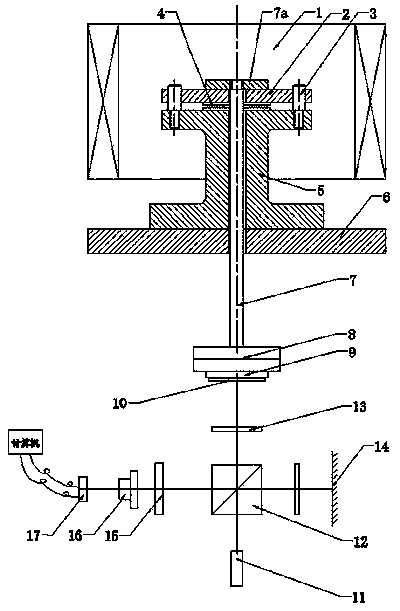
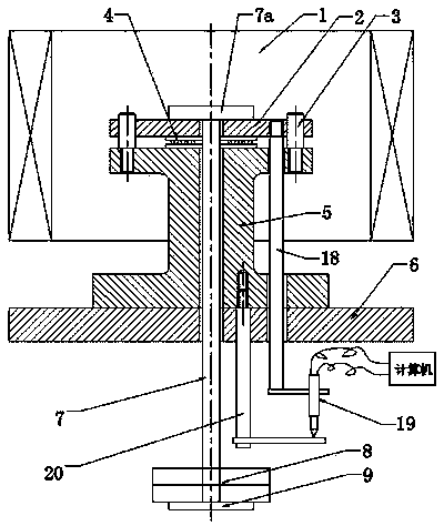
[0021] figure 1 The working principle diagram of a test device for measuring the compressive creep performance of solder joints in microelectronic packages is shown. combine figure 2 , 3 , the test device for measuring the compression creep performance of solder joints in microelectronic packaging consists of a device main body and peripheral equipment. The device main body includes an environmental chamber 1, a sample stage 5 and a loading mechanism, and the upper half of the sample stage 5 is arranged in the environmental chamber 1. The lower part of the sample table 5 is fixedly connected with the support table 6, and the sample 4 is placed on the upper plane of the sample table 5, and the sample 4 is pressed down with the upper pressing plate 2, and uniformly distributed and fixed on the sample table 5 are arranged on the periphery of the upper pressing plate 2. The guide hole that the positioning pin 3 of the upper part matches. The loading mechanism adopts the load r...


PUM

PropertyMeasurementUnit
melting pointaaaaaaaaaa

Abstract

The invention discloses a testing device for determining compression creepage performance of microelectronic packing welding spots, belonging to the field of testing on the mechanical performance of materials. A main body of the testing device comprises an environmental box, a sample stand, a locating mechanism and a loading mechanism, wherein the upper half part of the sample stand is arranged in the environmental box, a load rod of the loading mechanism is fixedly connected with a supporting disc after sequentially penetrating through a supporting table top, the sample stand, a test sample and an upper pressure plate, and a weight tray is arranged at the lower part of the load rod. In testing, the environment box enables the test sample to reach an experimental temperature, the loading mechanism applies pressure stress load to the test sample, and an optical displacement meter mechanism or an LVDT (Linear Variable Differential Transformer) displacement meter mechanism is used for recording the displacement variation of the test sample in testing. The testing device enables the test sample to be located accurately and loaded uniformly, and the experiment accuracy can be improved. The working conditions of the microelectronic packing welding spots under conditions of different temperatures and pressure loads can be simulated through regulating the temperature of the environmental box and the number of loaded weights so as to obtain creepage data under corresponding working conditions, and especially, the testing device can meet testing demands of practical microelectronic products in production.

Description

technical field [0001] The invention relates to a test device for measuring the compressive creep performance of solder joints in microelectronic packaging, belonging to the field of mechanical performance testing of materials. Background technique [0002] Metal materials will creep when they are more than 0.5 times the absolute temperature of the melting point and under load. To evaluate the high-temperature mechanical properties of metal materials, the influence of creep deformation on the mechanical properties of materials must be considered. Especially in the field of microelectronic packaging, creep is important for soldering. The impact on point mechanical properties and reliability is critical. Because the melting point of solder commonly used in microelectronic packaging is generally lower than 230°C, even at room temperature it has exceeded 0.5 times the absolute temperature of the melting point of the solder alloy. For example, the melting point of the eutectic al...

Claims


Application Information

Patent Timeline
Patent Type & Authority Applications(China)
IPC IPC(8): G01N3/14G01B11/16
Inventor 黄明亮赵宁马海涛赵杰杨耀春张飞
Owner DALIAN UNIV OF TECH
Why Eureka
Try Eureka