Semiconductor device and manufacturing method thereof

A semiconductor and device technology, applied in the field of semiconductor devices and their manufacturing, can solve problems such as electromigration, device failure, high resistance, etc.

Active Publication Date: 2016-11-30
TAIWAN SEMICON MFG CO LTD
View PDF3 Cites 0 Cited by
  • Summary
  • Abstract
  • Description
  • Claims
  • Application Information

AI Technical Summary

Problems solved by technology

The problem of electromigration or high resistance occurs due to the reduced size of the wire, which increases the resistance of the wire and can cause device failure

Method used


Image

  • Semiconductor device and manufacturing method thereof
  • Semiconductor device and manufacturing method thereof
  • Semiconductor device and manufacturing method thereof

Examples


Embodiment Construction

[0035] The making and using of embodiments of the invention are discussed in detail below. It should be appreciated, however, that the present invention provides many applicable inventive concepts that can be embodied in a wide variety of specific contexts. The specific embodiments discussed are merely illustrative specific ways to make and use the embodiments, and do not limit the scope of the embodiments.

[0036] Embodiments of the invention relate to methods of designing and manufacturing conductive components for semiconductor devices. This article will describe a new approach to the design and fabrication of conductive components for semiconductor devices.

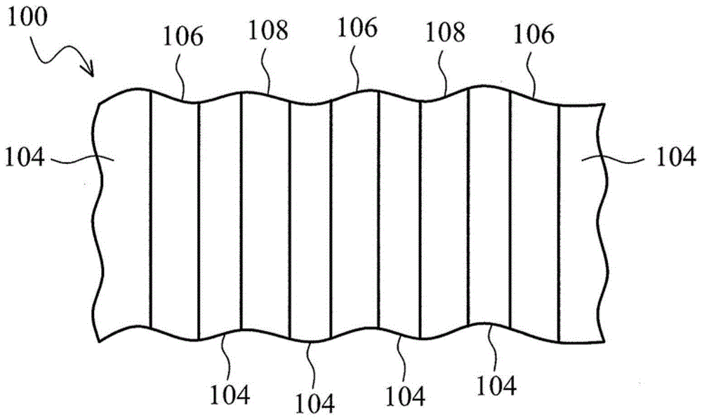
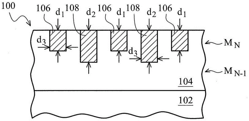
[0037] figure 1 is a top view of a semiconductor device 100 according to an embodiment of the present invention. figure 2 yes figure 1 A cross-sectional view of the semiconductor device 100 shown in . Semiconductor device 100 includes workpiece 102 . For example, workpiece 102 may include a semiconductor subst...


PUM


Abstract

A semiconductor device and method of manufacturing the same are disclosed. In one embodiment, a semiconductor device includes a workpiece and a plurality of first conductive lines disposed over the workpiece and in a metallization layer. A plurality of second conductive lines are disposed over the workpiece and in the metallization layer. In the cross section of the workpiece, the vertical height of the plurality of second conductive wires is greater than the vertical height of the plurality of first conductive wires.

Description

technical field [0001] The present invention relates to a semiconductor device and a method of manufacturing the same. Background technique [0002] Semiconductor devices are used in a variety of electronic applications such as personal computers, cell phones, digital cameras, and other electronic equipment. Usually semiconductor devices are manufactured by sequentially depositing various insulating or dielectric layers, conductive layers, and semiconducting material layers over a semiconductor substrate, and patterning the various material layers using photolithography to form circuit components and element. [0003] The semiconductor industry continues to increase the integration density of various electronic components (eg, transistors, diodes, resistors, capacitors, etc.) by continuously reducing the minimum component size so that more components can be integrated into a given area. As the size of the wires decreases, the problem of electromigration or high resistance ...

Claims


Application Information

Patent Timeline
Patent Type & Authority Patents(China)
IPC IPC(8): H01L23/538H01L21/768
Inventor 傅宗民陈文豪陈殿豪
Owner TAIWAN SEMICON MFG CO LTD
Why Eureka
Try Eureka