Pixel structure, array substrate, display device and manufacturing method of pixel structure

A technology of pixel structure and manufacturing method, which is applied in the field of pixel structure, display device and pixel structure manufacturing, and array substrate, and can solve the problem of inconsistency between the diameter of the first via hole and the second via hole, and the difference between the second transparent electrode layer and the source-drain electrode. Layer disconnection, lateral etching of the first passivation layer 5, etc.

Active Publication Date: 2014-01-22
BOE TECH GRP CO LTD
View PDF3 Cites 7 Cited by
  • Summary
  • Abstract
  • Description
  • Claims
  • Application Information

AI Technical Summary

Problems solved by technology

[0004] The inventors of the present application found that, in the process of manufacturing the pixel structure of the above-mentioned array substrate, the first via hole formed on the first passivation layer 5 and the second via hole formed on the resin layer 6 respectively through the patterning process When the first passivation layer 5 is etched laterally, the diameter of the first via hole and the second via hole will be inconsistent; thus, the second transparent electrode layer will be disconnected from the source and drain layers. ,like figure 1 The second transparent electrode layer 9 shown in the middle area A is disconnected from the source and drain layer 4, thereby affecting the quality of the array substrate

Method used


Image

  • Pixel structure, array substrate, display device and manufacturing method of pixel structure
  • Pixel structure, array substrate, display device and manufacturing method of pixel structure
  • Pixel structure, array substrate, display device and manufacturing method of pixel structure

Examples


Embodiment Construction

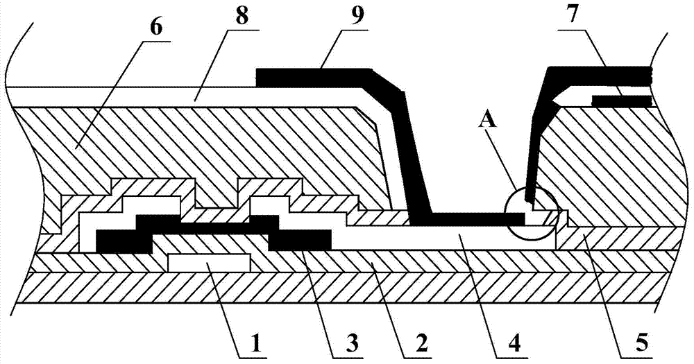
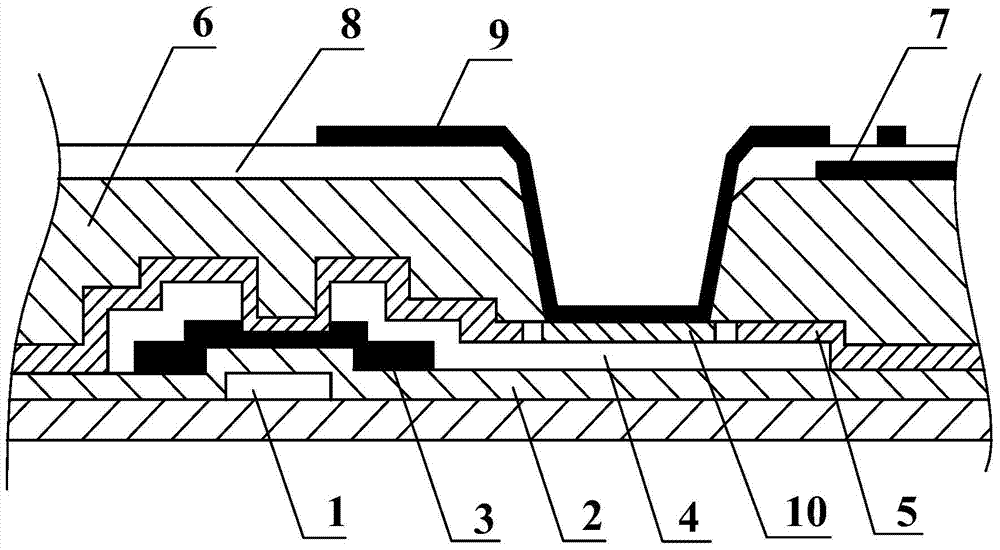
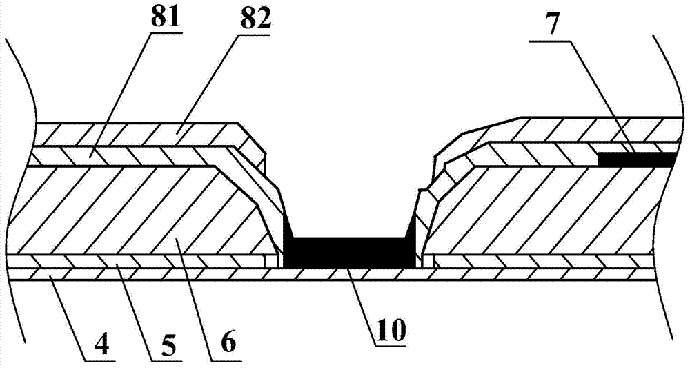
[0069] In order to reduce the probability that the second transparent electrode layer is disconnected from the source-drain layer and improve the quality of the array substrate, the present invention provides a pixel structure. By adding a conductive compensation block in the first via hole, the second transparent electrode Layer is electrically connected to the source and drain layer through the conductive compensation block, so as to reduce the probability of disconnection of the second transparent electrode layer deposited in the first via hole, that is, to reduce the disconnection of the second transparent electrode layer and the source and drain layer chance, thereby improving the quality of the array substrate.

[0070] In order to enable those skilled in the art to better understand the technical solutions of the present invention, the embodiments of the present invention will be described in detail below in conjunction with the accompanying drawings.

[0071] Such as ...


PUM


Abstract

The invention relates to the technical field of display panel manufacture, in particular to a pixel structure, an array substrate, a display device and a manufacturing method of the pixel structure, and aims to reduce the disconnection probability between a second transparent electrode layer and a source drain electrode layer and improve the quality of the array substrate. The pixel structure comprises a substrate provided with the source drain electrode layer, a first passivation layer covering the source drain electrode layer and provided with a first via hole, a resin layer covering the first passivation layer and provided with a second via hole, a first transparent electrode layer arranged on the resin layer, a second passivation layer covering the resin layer and the first transparent electrode layer and provided with a third via hole, a conductive compensation block arranged in the first via hole, and the second transparent electrode layer arranged on the second passivation layer and in the third via hole, the second via hole and the first via hole. The second transparent electrode layer is electrically connected with the source drain electrode layer through the conductive compensation block.

Description

technical field [0001] The present invention relates to the technical field of display panel manufacturing, in particular to a pixel structure, an array substrate, a display device and a method for manufacturing the pixel structure. Background technique [0002] At present, high resolution is a major development trend of the display panel. When the resolution of the display panel is increased from 200 pixels per inch (pixels per inch, hereinafter referred to as ppi) to 300Pppi, 400ppi, 500ppi or more than 500ppi, due to the The reduction of the distance between them leads to a sharp decrease in the aperture ratio. Therefore, an array substrate manufactured by eight patterning processes has emerged, which can effectively compensate the aperture ratio. [0003] Such as figure 1 Shown is a structural schematic diagram of a pixel structure in the prior art. The pixel structure includes: a base substrate, a gate layer 1 disposed on the base substrate, a gate insulating layer 2 ...

Claims


Application Information

Patent Timeline
Patent Type & Authority Applications(China)
IPC IPC(8): H01L27/12H01L21/77
CPCG02F1/136227H01L27/124
Inventor 曹占锋谷敬霞姚琪张峰丁录科
Owner BOE TECH GRP CO LTD
Why Eureka
Try Eureka