

High-light effect and high-power integrated LED with even light spots
A high-efficiency, high-power technology, used in semiconductor devices, electrical components, circuits, etc., can solve the problems of light spot generation, uneven and thorough phosphor excitation, poor heat dissipation, etc., to achieve high excitation efficiency, increased brightness, and quality reliability. boosted effect
Inactive Publication Date: 2014-02-05
山东光因照明科技有限公司
View PDF4 Cites 56 Cited by
- Summary
- Abstract
- Description
- Claims
- Application Information
AI Technical Summary
Problems solved by technology
Method used
View moreImage
Smart ImageViewing Examples

Examples
Embodiment Construction
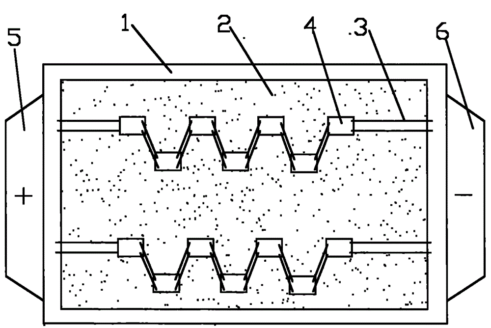
[0010] like figure 2 As shown, a high-efficiency and high-power integrated LED with uniform light spot is mainly composed of a bracket 1, a gold wire 3 and a number of chips 4. The chips 4 are fixed on the bracket 1, and the chips 4 are connected by gold wires 3. The chips at both ends 4. Connect the positive pole 5 and the negative pole 6 of the bracket 1 through the gold wire 3, the chip 4 is evenly distributed on the surface of the bracket 1 according to the S-shaped structure, and the bowl of the bracket 1 is filled with fluorescent glue 2.
Login to View More PUM
 Abstract
A high-light effect and high-power integrated LED with even light spots is mainly composed of a support, gold wires and a plurality of wafers. The wafers are fixed on the support and are connected through the gold wires. The wafers at the two ends are connected with the positive electrode of the support and the negative electrode of the support through the gold wires, the wafers are evenly distributed on the surface of the support in an S-shaped structure mode, and a bowl cup of the support is filled with fluorescence glue. According to the high-light effect and high-power integrated LED with the even light spots, the S-type crystal solid wire method is adopted, the wafers are evenly distributed on the surface of the support, the bowl cup of the support is filled with the fluorescence glue, and therefore an LED can emit even light without a light spot, the excitation efficiency of fluorescent powder is higher, and the brightness is greatly improved. Due to the fact that the wafers are arranged in a scattered mode, the heat dissipation of the high-light effect and high-power integrated LED is better, and the quality reliability is enhanced.
Description
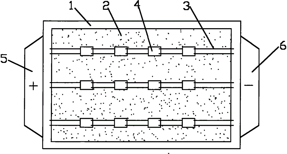
technical field [0001] The invention relates to the technical field of lighting fixtures, in particular to a high-efficiency and high-power integrated LED with uniform light spots. Background technique [0002] At present, the main structure of high-power integrated LED is composed of: bracket, chip, gold wire, phosphor (only available in white light), and AB glue, such as figure 1 As shown, a plurality of LED chips (4) are fixed on the bracket (1) by silver glue, the LED chips (4) are connected to each other by gold wires (3), and the LED chips (4) at both ends are connected by gold wires (3) It is connected to the support positive pole 5 and the support negative pole 6 of the support (1), wherein the cup of the support (1) is provided with silica gel filled between a plurality of LED chips (4), and wraps the gold wire (3). The structure of the LED can prevent the damage of some gold wires or LED chips inside the LED integrated light source, and solve the phenomenon that t...
Claims
Login to View More Application Information
Patent Timeline
 IPC IPC(8): H01L25/075H01L33/48H01L33/50H01L33/64
CPCH01L2224/48137H01L2224/49111
Inventor李登延
Owner山东光因照明科技有限公司