

Improved LED packaging method and packaging structure
A technology of LED encapsulation and encapsulation method, which is applied in the direction of electrical components, circuits, semiconductor devices, etc., can solve problems such as high cost and complicated operation, and achieve low cost, broad application prospects, and the effect of improving luminous brightness and heat dissipation performance
- Summary
- Abstract
- Description
- Claims
- Application Information
AI Technical Summary
Problems solved by technology
Method used
Image

Examples
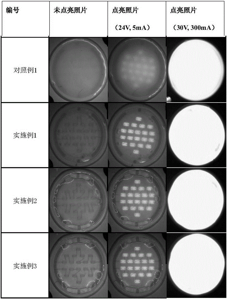
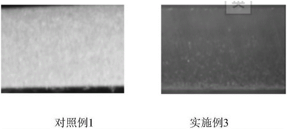
Embodiment 1
[0084] The LED packaging method of Example 1 includes: injecting the mixture of phosphor powder and organic silica gel into the chip holder that has completed the crystal bonding and gold wire binding by dispensing, completing the phosphor powder coating on the surface of the LED chip, and then heating the LED chip at temperature Stand in an environment of 60°C for 2 hours (this operation can be done on a heating platform), and finally cure at a temperature of 150°C for 4 hours.
[0085] The LED packaging methods of Examples 2 and 3 are basically the same, including: injecting the mixture of phosphor powder and organic silica gel into the chip holder that has completed the crystal bonding and gold wire binding by dispensing, and completing the phosphor powder coating on the surface of the LED chip. Cover, then let it stand for 2 hours in an environment with a temperature of 60°C (this operation can be done on a heating platform), then let it stand for 1 hour in an environment w...
PUM
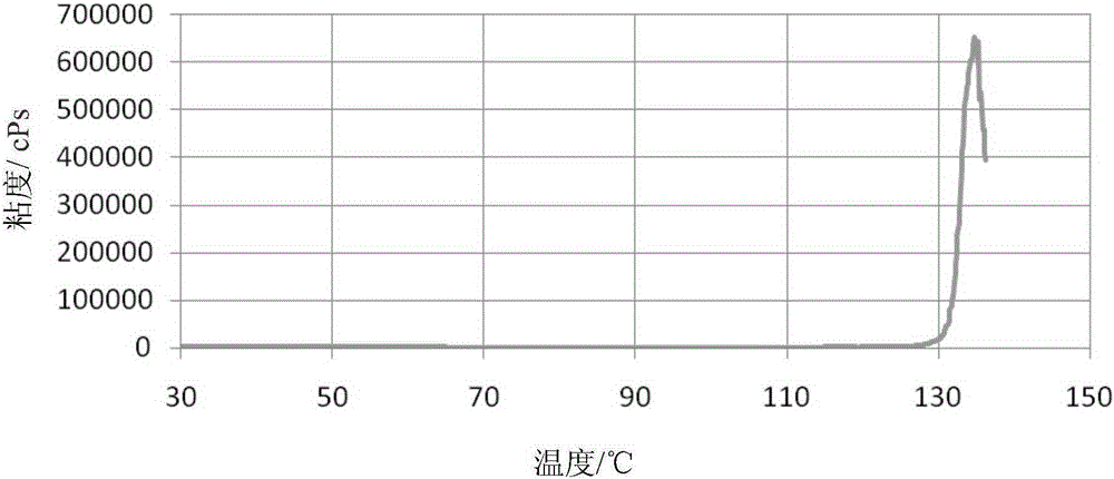
| Property | Measurement | Unit |
|---|---|---|
| Viscosity | aaaaa | aaaaa |
| Thickness | aaaaa | aaaaa |
| Viscosity | aaaaa | aaaaa |
Abstract
Description
Claims
Application Information