Semiconductor device and manufacturing method thereof

A technology of semiconductors and conductors, which is applied in the field of semiconductor devices with high gate coupling value and its production, which can solve the problems of flash memory unit size reduction and reduction, and achieve the effect of stabilizing the capacitance value

Active Publication Date: 2018-03-27
UNITED MICROELECTRONICS CORP
View PDF4 Cites 0 Cited by
  • Summary
  • Abstract
  • Description
  • Claims
  • Application Information

AI Technical Summary

Problems solved by technology

[0003] However, due to the miniaturization trend of electronic products, the size of flash memory cells is reduced, resulting in a decrease in gate coupling ratio (GCR)

Method used


Image

  • Semiconductor device and manufacturing method thereof
  • Semiconductor device and manufacturing method thereof
  • Semiconductor device and manufacturing method thereof

Examples


Embodiment Construction

[0047] In order to enable those who are familiar with the technical field of the present invention to further understand the present invention, the preferred embodiments of the present invention are listed below, together with the accompanying drawings, to describe in detail the composition of the present invention and the desired effects .

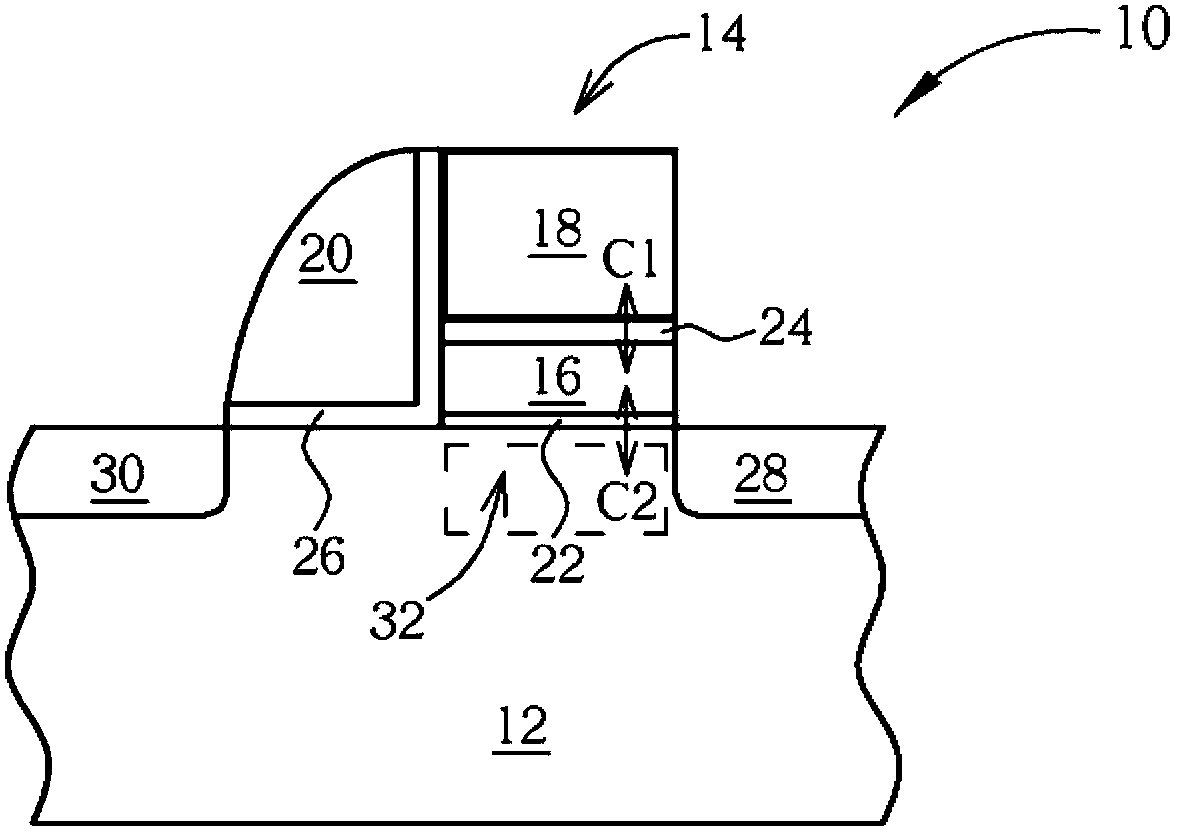
[0048] Please refer to figure 1 . figure 1 A schematic cross-sectional view of a semiconductor device according to an embodiment of the present invention is shown. Such as figure 1 As shown, the semiconductor device 10, taking a flash memory unit as an example, includes a semiconductor substrate 12, a gate stack 14 disposed on the semiconductor substrate 12, and a select gate (select gate) 20 disposed on the gate stack 14 Side, wherein the gate stack 14 includes a floating gate (floating gate) 16 and a control gate (control gate) 18 . The semiconductor substrate 12 may include, for example, a substrate made of silicon, gallium arsenid...


PUM


Abstract

The invention discloses a semiconductor device and a manufacturing method thereof. The semiconductor device comprises a semiconductor substrate, two floating gates, one control gate and a first dielectric layer. The floating gates are arranged on the semiconductor substrate, the control gate is partially overlapped with the floating gates, and a part of the control gate is located between the floating gates. In addition, the thickness of the first dielectric layer arranged between the floating gates and the control gate is fixed.

Description

technical field [0001] The present invention relates to a semiconductor device and a manufacturing method thereof, in particular to a semiconductor device with a high gate coupling ratio (GCR) and a manufacturing method thereof. Background technique [0002] Flash memory (flash memory) is a kind of non-volatile (non-volatile) memory, which can save the information content stored in the memory even when there is no external power supply. In recent years, flash memory has been widely used in mobile phones, digital cameras, video players, Personal digital assistant (personal digital assistant, PDA) and other electronic products or developing system single chip (system on a chip, SOC). [0003] However, due to the miniaturization trend of electronic products, the size of the flash memory unit is reduced, resulting in a decrease in gate coupling ratio (GCR). Therefore, how to increase the gate coupling value so as to improve the electrical performance of the flash memory unit i...

Claims


Application Information

Patent Timeline
Patent Type & Authority Patents(China)
IPC IPC(8): H01L29/788H01L29/423H01L21/336
CPCH01L29/42324H01L29/66825H01L29/788
Inventor 许正源任驰温增飞
Owner UNITED MICROELECTRONICS CORP
Why Eureka
Try Eureka