

Piezoelectric element
A technology of piezoelectric elements and piezoelectric layers, applied in the field of piezoelectric elements, to achieve the effect of easy polarization treatment
- Summary
- Abstract
- Description
- Claims
- Application Information
AI Technical Summary
Problems solved by technology
Method used
Image

Examples
no. 1 Embodiment approach ]
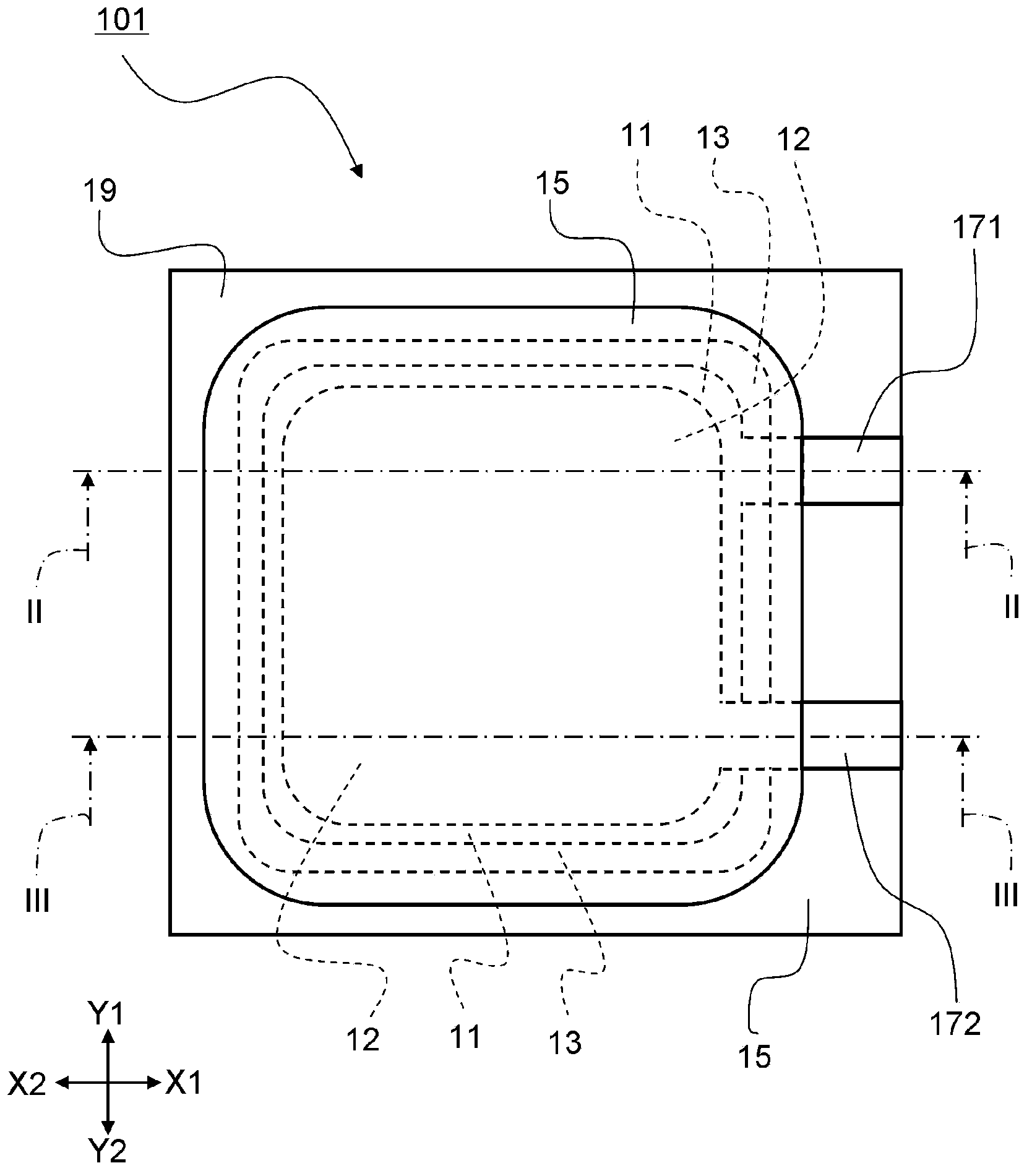
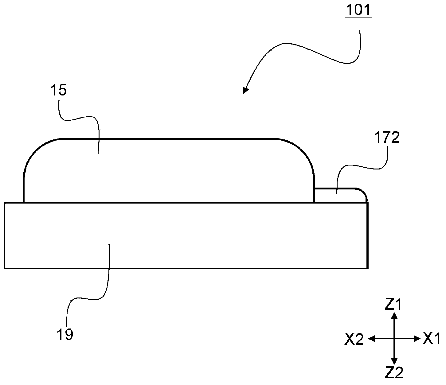
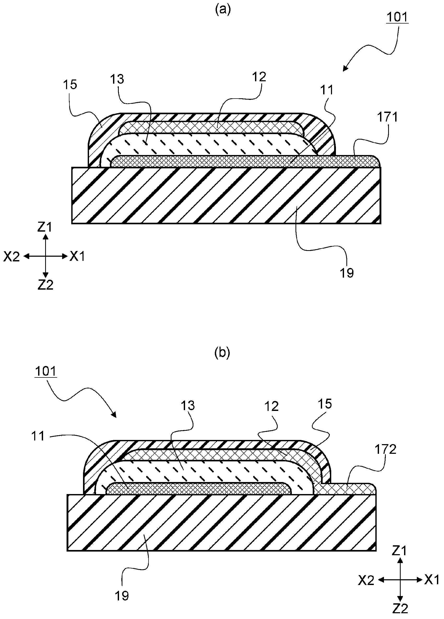
[0047] figure 1 It is a configuration diagram illustrating the piezoelectric element 101 according to the first embodiment of the present invention, and is a plan view thereof. figure 2 It is a configuration diagram for explaining the piezoelectric element 101 according to the first embodiment of the present invention, from figure 1 Side view of Y2 side view shown. image 3 It is a figure explaining the piezoelectric element 101 of 1st Embodiment of this invention, image 3 (a) is figure 1 The sectional view at the line II-II shown, image 3 (b) is figure 1 Sectional view at line III-III shown. also, Figure 1 to Figure 3 This is a structural diagram for easy explanation, so the dimensions in the thickness direction (Z1-Z2 direction) are greatly different from the actual ones.
[0048] The piezoelectric element 101 according to the first embodiment of the present invention is as Figure 1 to Figure 3 As shown, a first electrode layer 11 laminated on a flexible sub...
no. 2 Embodiment approach ]
[0086] Figure 7 It is a configuration diagram illustrating the piezoelectric element 102 according to the second embodiment of the present invention, and is a plan view thereof. Figure 8 It is a configuration diagram illustrating the piezoelectric element 102 according to the second embodiment of the present invention, from Figure 7 Side view of Y2 side view shown. Figure 9 It is a figure explaining the piezoelectric element 102 of 2nd Embodiment of this invention, Figure 9 (a) is Figure 7 Sectional view at line IX-IX shown, Figure 9 (b) is Figure 7 Sectional view at line X-X shown. The piezoelectric element 102 of the second embodiment differs from the first embodiment in that piezoelectric layers ( 23A, 23B) are provided on both surfaces of a substrate 29 . In addition, the same code|symbol is attached|subjected to the same structure as 1st Embodiment, and detailed description is abbreviate|omitted. in addition, Figure 7 to Figure 9 This is a structural diag...
Deformed example 1
[0112] In the above-mentioned first embodiment, the conductive silver-containing phenolic resin is preferably used for the second electrode layer 12 , but the conductive member and synthetic resin used for the first electrode layer 11 may also be used.
PUM
 Abstract
Description
Claims
Application Information