Bipolar pnp transistor and method of manufacturing the same

A manufacturing method and transistor technology, which are applied in transistors, semiconductor/solid-state device manufacturing, semiconductor devices, etc., can solve the problem of non-adjustable magnification of small current, and achieve the effect of adjustable magnification of small current.

Active Publication Date: 2017-02-08
CHENGDU SILAN SEMICON MFG
View PDF5 Cites 0 Cited by
  • Summary
  • Abstract
  • Description
  • Claims
  • Application Information

AI Technical Summary

Problems solved by technology

[0007] The purpose of the present invention is to provide a bipolar PNP transistor and its manufacturing method, to solve the problem that the small current magnification of the existing bipolar PNP transistor cannot be adjusted

Method used


Image

  • Bipolar pnp transistor and method of manufacturing the same
  • Bipolar pnp transistor and method of manufacturing the same
  • Bipolar pnp transistor and method of manufacturing the same

Examples


Embodiment Construction

[0039] The bipolar PNP transistor and its manufacturing method proposed by the present invention will be further described in detail below with reference to the drawings and specific embodiments. Advantages and features of the present invention will be apparent from the following description and claims. It should be noted that all the drawings are in a very simplified form and use imprecise scales, and are only used to facilitate and clearly assist the purpose of illustrating the embodiments of the present invention.

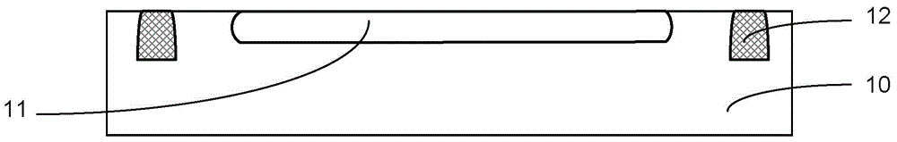
[0040] Please refer to Figure 13 , which is a schematic structural diagram of a bipolar PNP transistor according to an embodiment of the present invention. Such as Figure 13 As shown, the bipolar PNP transistor 100 includes: a substrate 10; an epitaxial layer 13 formed on the substrate 10; a deep phosphorus region 14, a base region 16, and a collector region formed in the epitaxial layer 13 17 and emission region 18; the first interlayer dielectric layer 19...


PUM


Abstract

The invention provides a bipolar PNP transistor and a manufacturing method thereof. The bipolar PNP transistor comprises a substrate, an epitaxial layer formed on the substrate, a deep phosphorus zone, a base zone, a collection zone and an emission zone which are formed in the epitaxial layer, a first interlayer dielectric layer and a voltage modulation dielectric layer which are formed on the epitaxial layer, a first interconnection line formed on the first interlayer dielectric layer and the voltage modulation dielectric layer, a second interlayer dielectric layer formed on the first interlayer dielectric layer and the first interconnection line, and a second interconnection line formed on the second interlayer dielectric layer, wherein the base zone is covered by the voltage modulation dielectric layer, and electric leading out is realized through the first interconnection line. According to the bipolar PNP transistor and the manufacturing method, through forming the voltage modulation dielectric layer on the base zone, the electric leading out of the voltage modulation dielectric layer is realized through the first interconnection line, so the charge concentration of a base zone surface is changed through changing the induction charge number of the voltage modulation dielectric layer, and thus the magnification times of small current is adjustable.

Description

technical field [0001] The invention relates to the field of integrated circuit manufacturing, in particular to a bipolar PNP transistor and a manufacturing method thereof. Background technique [0002] A photoelectric sensor is a sensor that converts light signals into electrical signals through photosensitive devices. At present, photosensitive devices are generally manufactured by semiconductor technology, including photodiodes, phototransistors and photoresistors. Since the light received by the photosensitive device is relatively weak, the photogenerated current generated is also relatively weak. Usually, a preamplifier circuit is required to cooperate with the photosensitive device to amplify the signal. The photosensitive device and the preamplifier circuit are integrated on one chip to form a photoelectric sensor. [0003] With the different applications of photoelectric sensors, various environmental disturbances have a great impact on photosensitive devices, such...

Claims


Application Information

Patent Timeline
Patent Type & Authority Patents(China)
IPC IPC(8): H01L29/73H01L29/10H01L21/331
CPCH01L29/0603H01L29/1004H01L29/66234H01L29/73
Inventor 李小锋张佼佼何金祥杨锐
Owner CHENGDU SILAN SEMICON MFG
Why Eureka
Try Eureka