PCB substrate stamping device
A technology for punching and substrates, applied in the field of PCB substrate punching devices, can solve the problems of surface insulation layer and hole insulation layer cracks, failure of withstand voltage performance, etc., to avoid bursting, improve yield and production efficiency, and remove hidden quality hazards. Effect
- Summary
- Abstract
- Description
- Claims
- Application Information
AI Technical Summary
Problems solved by technology
Method used
Image

Examples
Embodiment Construction
[0021] The embodiments of the present invention will be described in detail below with reference to the accompanying drawings, but the present invention can be implemented in many different ways defined and covered by the claims.
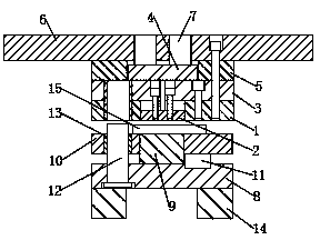
[0022] Please refer to figure 1 , the present invention provides a punching device for a PCB substrate (especially a double-sided sandwich aluminum substrate), comprising: a fixed lower mold part and an upper mold part that moves relative to the lower mold part; the upper mold part includes shearing plates 1, The upper mold core 2 and the upper mold ejection mechanism; the shearing plate 1 includes a cavity, and the upper mold core 2 is movably arranged in the cavity; the upper mold ejection mechanism drives the upper mold core 2 to move relative to the cavity towards the direction of the lower mold.
[0023] Please refer to figure 1 , when punching the board, the PCB substrate 15 is placed in the gap between the upper mold part and the lower mold ...
PUM
 Abstract
Description
Claims
Application Information