Wafer fixing device used in deposition film forming device

A wafer fixing and film forming device technology, applied in ion implantation plating, gaseous chemical plating, coating, etc., can solve problems such as smashing wafers, wafer 900 fragmentation, and increased risk of wafer fragmentation. Achieve the effect of avoiding sticking and good stability

Active Publication Date: 2014-03-26
WUXI CHINA RESOURCES HUAJING MICROELECTRONICS
View PDF9 Cites 12 Cited by
  • Summary
  • Abstract
  • Description
  • Claims
  • Application Information

AI Technical Summary

Problems solved by technology

[0007] in addition, figure 1 The shown wafer fixing device uses bumps 111 to act rigidly on the wafer, therefore, it is also easy to cause the wafer 900 to break when the ejector pin moves downward to fix and position the wafer 900; and the ceramic The positioning post 131 may also slip down abnormally and smash the wafer 900
Therefore, using figure 1 The wafer holding device 10 as shown also tends to increase the risk of wafer fragmentation when depositing and forming films

Method used


Image

  • Wafer fixing device used in deposition film forming device
  • Wafer fixing device used in deposition film forming device

Examples


Embodiment Construction

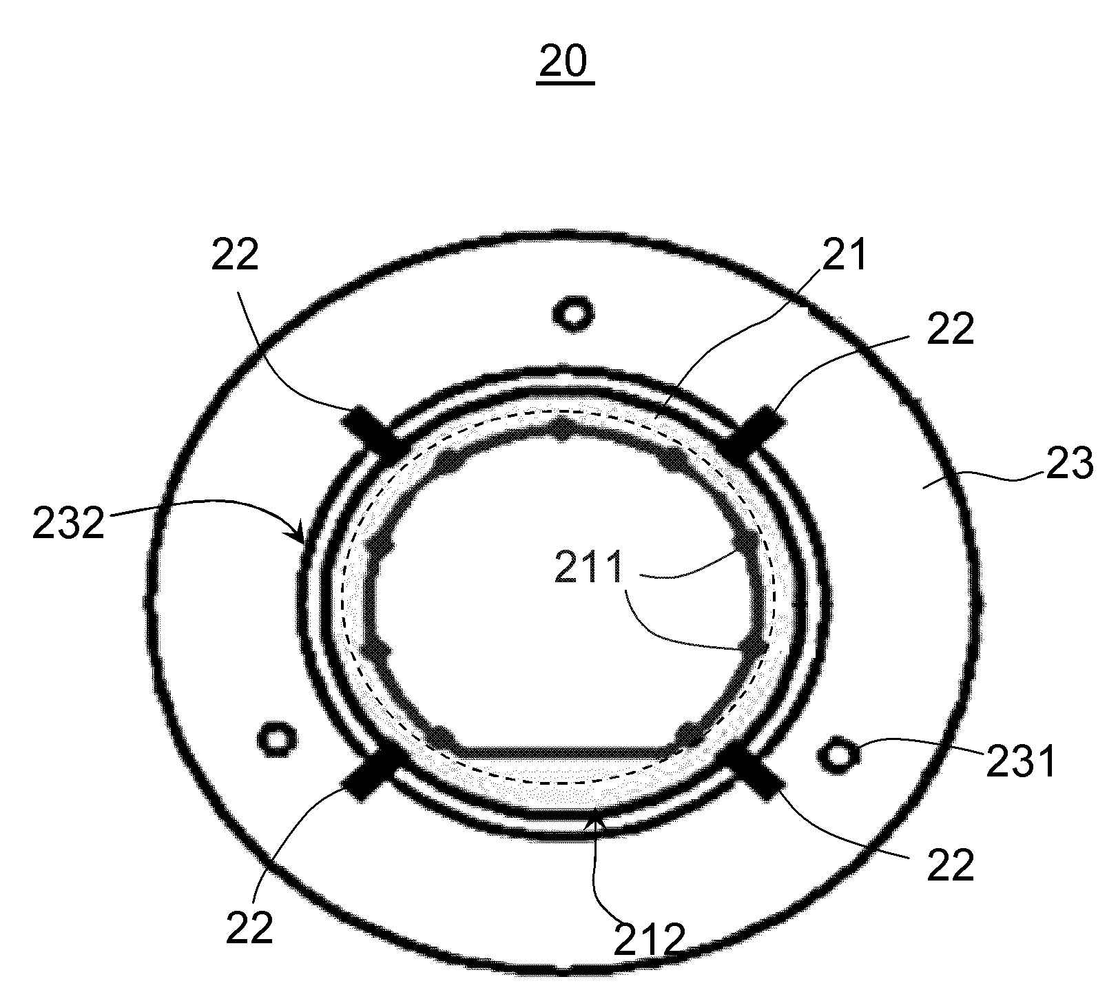
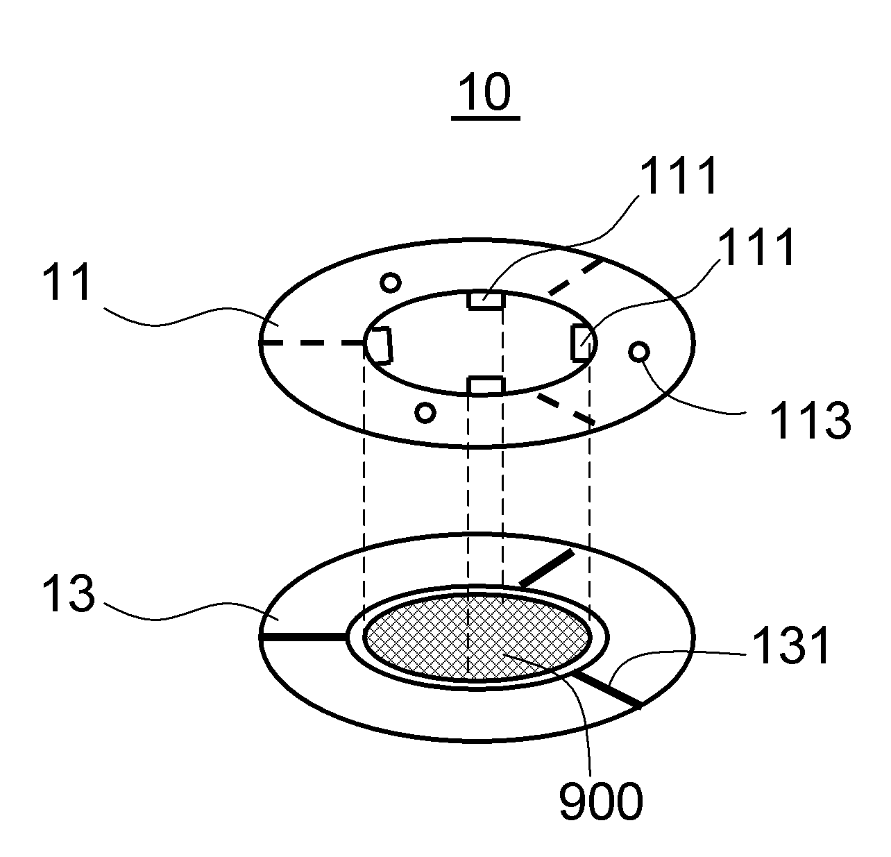
[0029] The following introduces some of the possible embodiments of the present invention, which are intended to provide a basic understanding of the present invention, but are not intended to identify key or decisive elements of the present invention or limit the scope of protection. It is easy to understand that, according to the technical solution of the present invention, those skilled in the art may propose other alternative implementation manners without changing the essence and spirit of the present invention. Therefore, the following specific embodiments and drawings are only exemplary descriptions of the technical solution of the present invention, and should not be regarded as the entirety of the present invention or as a limitation or restriction on the technical solution of the present invention.

[0030] In the following description, for clarity and conciseness of description, not all the various components shown in the figures are described. Directional terms use...


PUM


Abstract

The invention provides a wafer fixing device used in a deposition film forming device, belonging to the technical field of thin film deposition. The wafer fixing device comprises a positioning ring, a tabletting ring and an elastic fixing part for elastically fixing the tabletting ring on the positioning ring, wherein a plurality of tabletting points are formed on the surface facing the wafer, of the tabletting ring, and the tabletting points are applied to the upper surface of the wafer, so that the wafer is fixed related to a worktable of an inner cavity of the deposition film forming device. By using the wafer fixing device, the wafer breaking risk can be reduced and the wafer adhering phenomenon can be reduced.

Description

technical field [0001] The invention belongs to the technical field of thin film deposition, and relates to a wafer fixing device used in deposition and film forming devices. Background technique [0002] In the field of semiconductor manufacturing technology, various deposition and film formation technologies are widely used to pattern various thin film layers on wafers (Wafer) to manufacture chips containing complex circuits. Among them, a deposition and film forming device must be used in the thin film deposition process, for example, a PVD (Physical Vapor Deposition, physical vapor deposition) film forming device, a CVD (Chemical Vapor Deposition, chemical vapor deposition) film forming device. In the process of film formation (that is, film formation), it is usually necessary to fix the wafer on a workbench such as a heater (Heater) for film deposition. Therefore, in the deposition and film formation device, a wafer holding device is usually used . [0003] figure 1 ...

Claims


Application Information

Patent Timeline
Patent Type & Authority Applications(China)
IPC IPC(8): C23C14/50C23C16/458
Inventor 吉金林乐天贵陆雁华
Owner WUXI CHINA RESOURCES HUAJING MICROELECTRONICS
Why Eureka
Try Eureka