Stress dispersion MEMS (Micro-Electro-Mechanical Systems) plastic package pressure sensor and preparation method thereof

A pressure sensor, pressure technology, applied in the measurement of the property force of piezoelectric resistance materials, fluid pressure measurement by changing ohmic resistance, instruments, etc., to ensure complete and normal performance, improve reliability, and relatively small volume Effect

Active Publication Date: 2014-03-26
安徽京芯传感科技有限公司
View PDF8 Cites 23 Cited by
  • Summary
  • Abstract
  • Description
  • Claims
  • Application Information

AI Technical Summary

Problems solved by technology

[0003] Although the microelectronic packaging in the prior art provides protection for the pressure chip in terms of electrical, thermal, optical and mechanical properties, it cannot meet the ever-increasing performance requirements, reliability, heat dissipation and power of the pressure chip at a certain cost. The need for functions such as allocation

Method used


Image

  • Stress dispersion MEMS (Micro-Electro-Mechanical Systems) plastic package pressure sensor and preparation method thereof
  • Stress dispersion MEMS (Micro-Electro-Mechanical Systems) plastic package pressure sensor and preparation method thereof
  • Stress dispersion MEMS (Micro-Electro-Mechanical Systems) plastic package pressure sensor and preparation method thereof

Examples


Embodiment 1

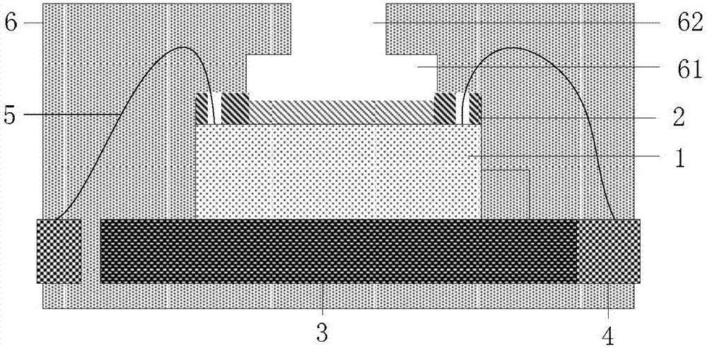
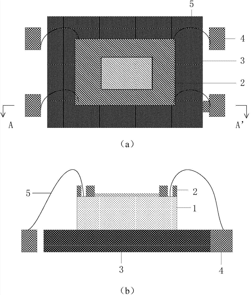
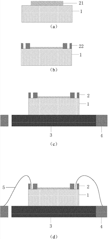
[0046] The plastic-encapsulated pressure sensor of this embodiment includes: a pressure chip 1, a pressure buffer layer 2, a substrate 3, a lead frame 4, a wire 5, and a plastic package 6; wherein, the upper surface of the pressure chip 1 is covered with a layer of soft rubber film to form a pressure buffer layer 2, and expose the welding points of the pressure chip and the wire; the lower surface of the pressure chip 1 is arranged on the substrate 3; the wire 4 connects the welding point of the pressure chip 1 with the lead frame 4, as figure 2As shown; the plastic package 6 encapsulates the pressure chip 1, the lead frame 4 and the substrate 3, and exposes the lead frame on the bottom surface or side of the plastic package; there is a cavity 61 between the plastic package 6 and the pressure buffer layer 2, and A through hole 62 is provided between the cavity 61 and the outer surface of the plastic package to communicate with the outside world, such as figure 1 shown. The p...

Embodiment 2

[0059] In this embodiment, the sealing film 8 is used to include the pressure chip 1 covered with the pressure buffer layer 2, the lead frame 4 and the substrate 3, and the bottom surface or the side surface of the lead frame is exposed, and the sealing film 8 is connected to the lead frame 4. Edge sealing; the plastic package body 6 encapsulates it outside the sealing film 8, thereby forming a cavity 61 between the plastic package body 6 and the pressure buffer layer 2, and opening a through hole 62, which is not sealed on the bottom surface or side of the plastic package body. Film-wrapped leadframes such as Figure 4 shown.


PUM

PropertyMeasurementUnit
thicknessaaaaaaaaaa
thicknessaaaaaaaaaa

Abstract

The invention discloses a stress dispersion MEMS (Micro-Electro-Mechanical Systems) plastic package pressure sensor and a preparation method thereof. The plastic package pressure sensor disclosed by the invention comprises a pressure chip, a pressure buffer layer, a base plate, a pin frame, conducting wires and a plastic package body, wherein a flexible glue thin film is covered on the upper surface of the pressure chip, and welding points of the pressure chip and the conducting wires are exposed to form the pressure buffer layer; a cavity is arranged between the plastic package body and the pressure buffer layer, and a through hole is formed between the cavity and the outer surface of the plastic package body and communicated with the outside. According to the stress dispersion MEMS plastic package pressure sensor and the preparation method thereof, the pressure buffer layer with the flexible glue thin film is adopted for covering a sensitive structure of the pressure chip, and the pressure during plastic injection is reduced through stress dispersion of the pressure buffer layer; moreover, the cavity with large area is arranged on the pressure buffer layer, and is beneficial to ventilating and radiating the pressure chip, so that the function that the performance of the pressure chip is complete and normal is ensured; the plastic package pressure sensor has the characteristics that the manufacturing technology is simple and advanced, the pressure chip is not influenced by stress, the performance is complete, the size is relatively smaller, the radiation is good, and the like.

Description

technical field [0001] The invention relates to microelectronic package technology, in particular to a stress dispersion MEMS plastic package pressure sensor and a preparation method thereof. Background technique [0002] The sensor package is a bridge connecting the sensor pressure chip and the electronic system. It usually refers to the module made of the sensor pressure chip and the substrate used to fix and protect it through thermosetting and thermoplastic materials. The connection between the silicon substrate of the pressure chip and the carrier or the shell is an important link not only for the integrated circuit but also for the sensor. [0003] Although the microelectronic packaging in the prior art provides protection for the pressure chip in terms of electrical, thermal, optical and mechanical properties, it cannot meet the ever-increasing performance requirements, reliability, heat dissipation and power of the pressure chip at a certain cost. Allocation and oth...

Claims


Application Information

Patent Timeline
Patent Type & Authority Applications(China)
IPC IPC(8): G01L9/06G01L1/18B81C3/00
Inventor 周浩楠张威苏卫国李宋陈广忠詹清颖张亚婷
Owner 安徽京芯传感科技有限公司
Why Eureka
Try Eureka