Method for Improving Gap Filling Ability of Pre-Metal Dielectric Layer

A technology of pre-metal dielectric layer and filling capability, applied in electrical components, electric solid-state devices, semiconductor/solid-state device manufacturing, etc., can solve problems such as uneven filling of materials and failure of semiconductor devices, reduce void defects, and improve filling capability. Effect

Active Publication Date: 2016-03-30
SEMICON MFG INT (SHANGHAI) CORP
View PDF3 Cites 0 Cited by
  • Summary
  • Abstract
  • Description
  • Claims
  • Application Information

AI Technical Summary

Problems solved by technology

[0009] It should be noted that for the rapidly developing sub-micron semiconductor devices, the distance between the gate and the gate is very narrow, mostly less than 10 nanometers, so in the previous step: the area between the gate and the gate When depositing the pre-metal dielectric layer, it is easy to cause uneven material filling and void defects. The void leads to the passage between the gate and the gate. If the conductive metal is filled inside, the conductive metal will just fill in the passage between the gate and the gate caused by the void, so that the gate and the gate are connected, and finally the semiconductor device will fail.

Method used


Image

  • Method for Improving Gap Filling Ability of Pre-Metal Dielectric Layer
  • Method for Improving Gap Filling Ability of Pre-Metal Dielectric Layer
  • Method for Improving Gap Filling Ability of Pre-Metal Dielectric Layer

Examples


Embodiment Construction

[0025] In order to make the object, technical solution and advantages of the present invention clearer, the present invention will be further described in detail below with reference to the accompanying drawings and examples.

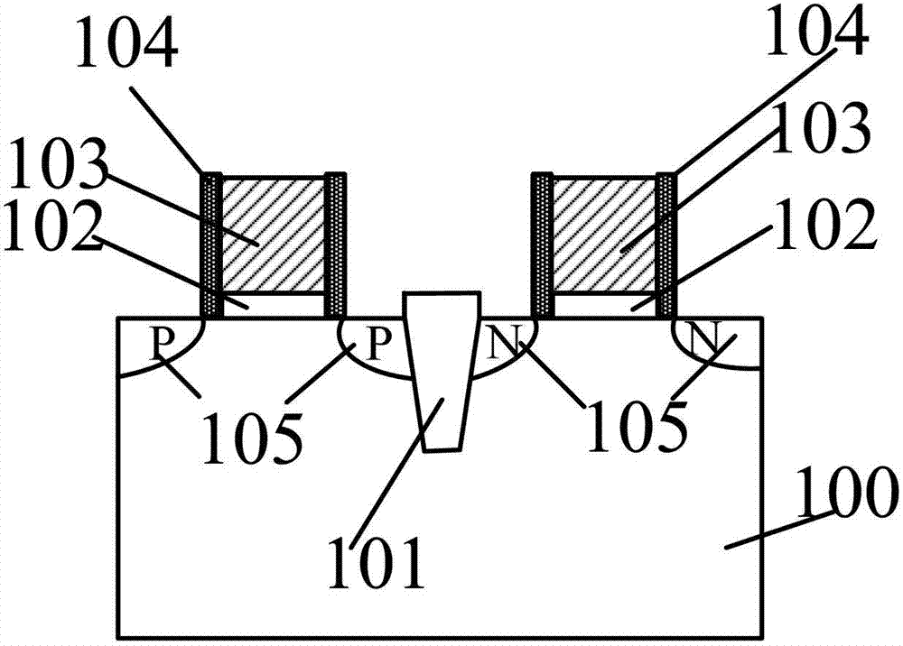
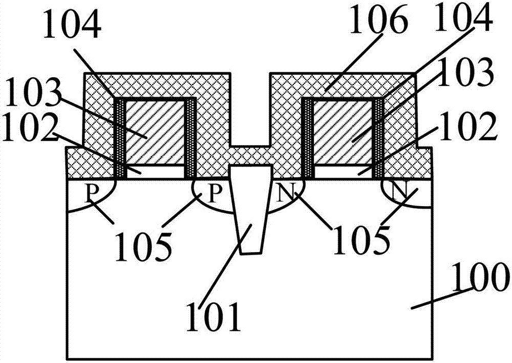
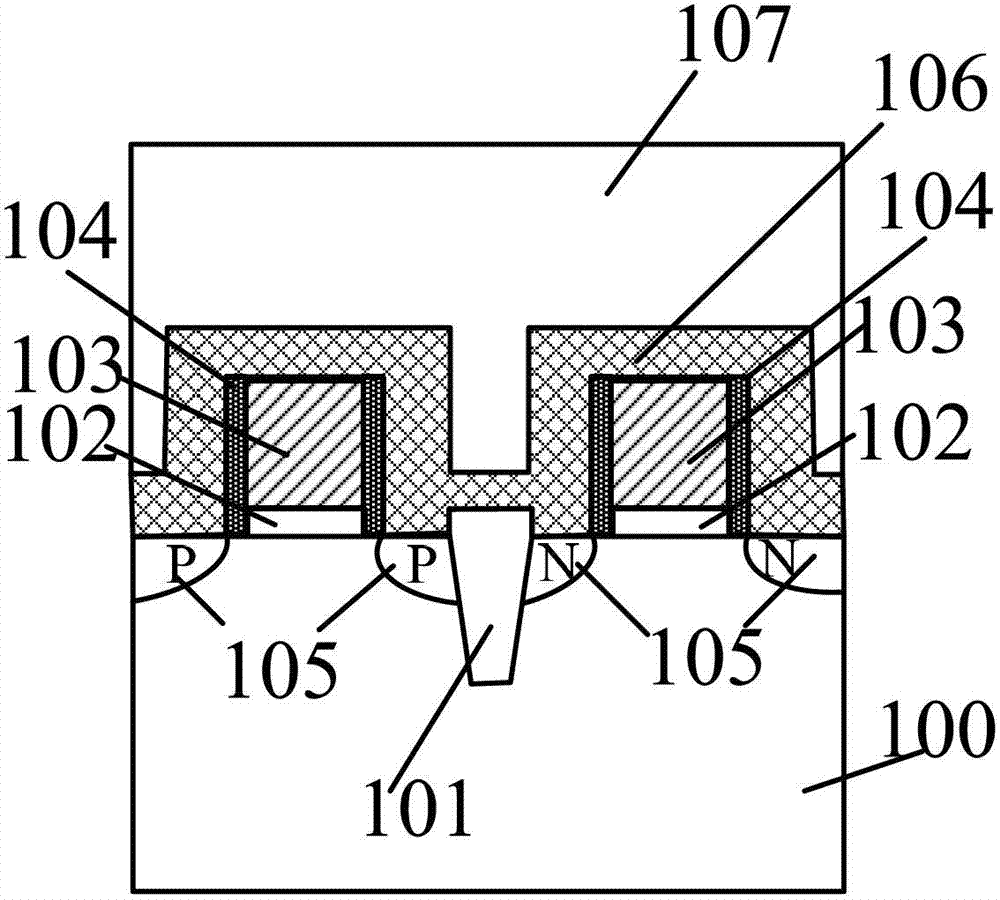
[0026] Studies have shown that under normal circumstances, the growth rate of the pre-metal dielectric layer on the surface of the silicon oxide layer is faster than that on the surface of the stressed silicon nitride layer, but after fluorine treatment on the surface of the stressed silicon nitride layer and the surface of the silicon oxide layer, the pre-metal layer The dielectric layer grows faster on the surface of the stressed silicon nitride layer than on the surface of the silicon oxide layer, so the present invention uses fluorine treatment to improve the growth selectivity ratio of the dielectric layer before the metal on the surface of the stressed silicon nitride layer and the surface of the silicon oxide layer, thereby Reach the object of the...


PUM


Abstract

The invention discloses a method for improving gap filling capability of a pre-metal dielectric. The method comprises the following steps: taking a shallow groove isolation area in a semiconductor substrate as a boundary, and forming a CMOS structure adopting a PMOS structure and an NMOS structure, wherein both the PMOS structure and the NMOS structure at least comprise gate oxides and polycrystalline silicon grid electrodes formed on the surface of the semiconductor substrate in sequence, side wall layers positioned on the two sides of the polycrystalline silicon grid electrodes and active areas positioned on the two sides of the polycrystalline silicon grid electrodes and in the semiconductor substrate; depositing a stress silicon nitride layer on the surface of the CMOS structure; depositing a silicon oxide layer on the surface of the stress silicon nitride layer, performing anisotropic etching, and reserving a silicon oxide layer on the side walls of the stress silicon nitride layer; performing fluorine treatment on the surfaces of the silicon oxide layer and the stress silicon nitride layer, and improving the growth selection ratio of the pre-metal dielectric on the surface of the stress silicon nitride layer and the surface of the silicon oxide layer; depositing the pre-metal dielectric. Through the adoption of the method, the defect that void is formed between the grid electrodes can be effectively overcome.

Description

technical field [0001] The invention relates to the fabrication technology of semiconductor devices, in particular to a method for improving the gap filling capability (gapfill) of a pre-metal dielectric layer (PMD). Background technique [0002] Currently, in the manufacture of semiconductor devices, silicon nitride can be used to induce stress in the transistor channel, thereby adjusting the carrier mobility in the channel. Complementary Metal-Oxide-Semiconductor (CMOS) structure includes NMOS structure and PMOS structure, the manufacturing method of CMOS structure in the prior art, combined with its specific cross-sectional structure schematic diagram, Figure 1a to Figure 1c Be explained. [0003] see Figure 1a , providing a semiconductor substrate 100, forming a shallow trench isolation region (STI) 101 on the semiconductor substrate 100, respectively forming a PMOS structure and an NMOS structure on both sides of the STI101 on the semiconductor substrate 100; specifi...

Claims


Application Information

Patent Timeline
Patent Type & Authority Patents(China)
IPC IPC(8): H01L21/768
CPCH01L21/76826H01L21/8238H01L2221/1005
Inventor 张彬邓浩
Owner SEMICON MFG INT (SHANGHAI) CORP
Why Eureka
Try Eureka