Display panel, manufacturing method thereof and display device

A technology for display panels and manufacturing methods, applied in semiconductor/solid-state device manufacturing, electrical components, electric solid-state devices, etc., can solve problems such as complex manufacturing process of color film substrates, poor display, etc., to ensure normal display, save production materials, The effect of reducing production costs

Active Publication Date: 2014-03-26
BOE TECH GRP CO LTD
View PDF4 Cites 8 Cited by
  • Summary
  • Abstract
  • Description
  • Claims
  • Application Information

AI Technical Summary

Problems solved by technology

It can be seen that the manufacturing process of the color filter substrate is relatively complicated, and because there are gaps on the flat protective layer 3, and the thickness of the transparent conductive layer 5 is very small, the transparent conductive layer 5 is easy to produce etching fractures, resulting in poor display

Method used


Image

  • Display panel, manufacturing method thereof and display device
  • Display panel, manufacturing method thereof and display device
  • Display panel, manufacturing method thereof and display device

Examples


Embodiment Construction

[0023] In order to make the technical problems, technical solutions and advantages to be solved by the embodiments of the present invention clearer, the following will describe in detail with reference to the drawings and specific embodiments.

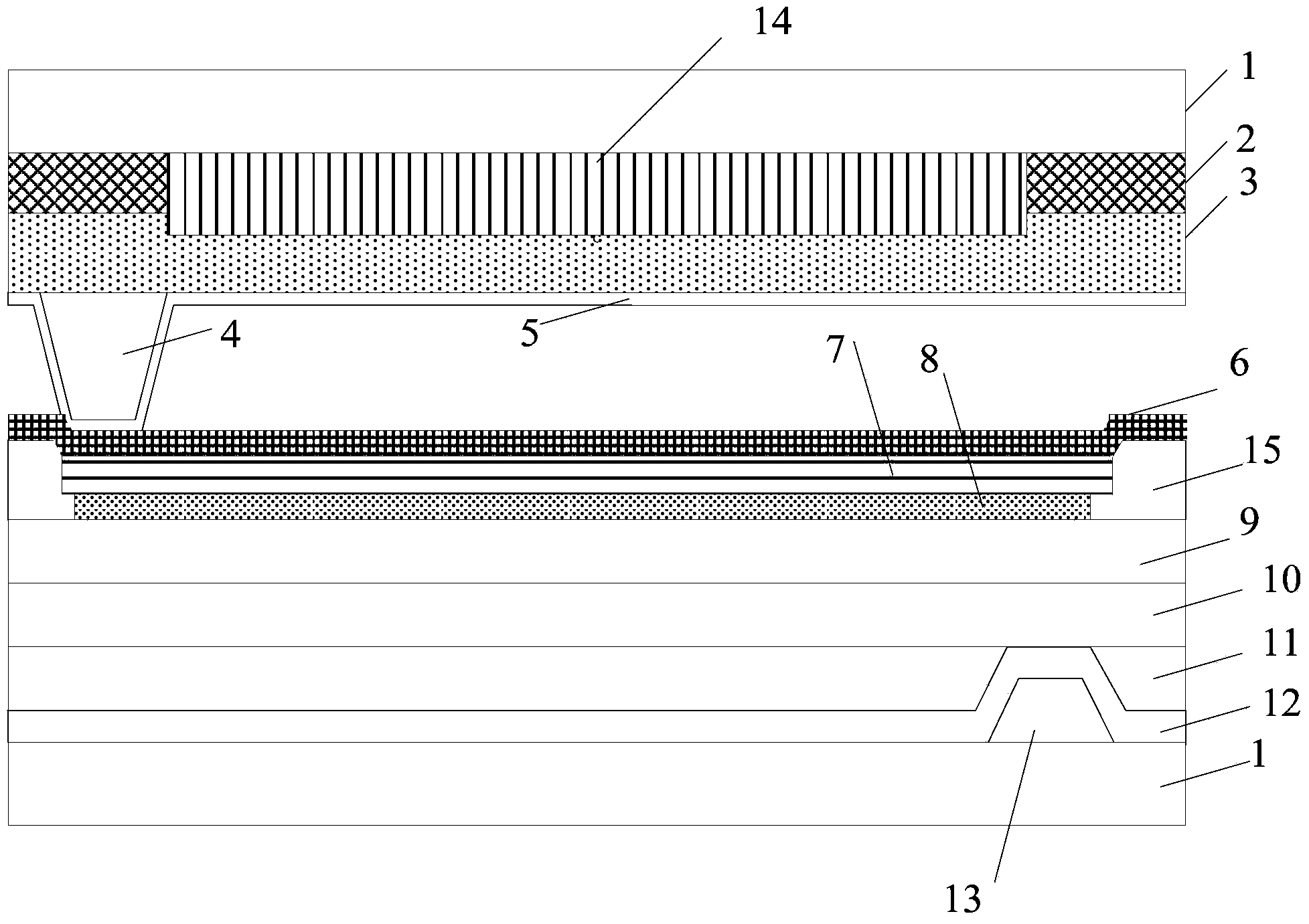
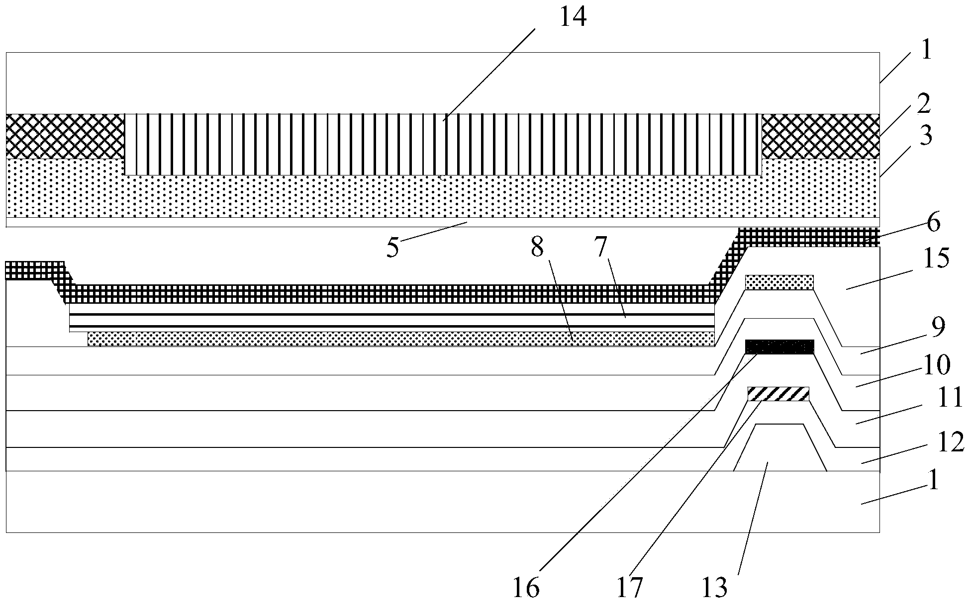
[0024] The embodiments of the present invention aim at the existing AMOLED display panel that needs to make columnar spacers on the color filter substrate, the process is relatively complicated, and it is easy to cause the problem of etching section and resistance change of the transparent conductive layer, and provides a display panel and The manufacturing method and the display device can save the manufacturing process of columnar spacers, thereby saving the production time and materials of the display panel, thereby reducing the production cost of the display panel, and ensuring that the transparent conductive layer on the color filter substrate does not Etched sections appear and the resistance is stable.

[0025] The display panel...


PUM


Abstract

The invention provides a display panel, a manufacturing method thereof and a display device, and belongs to the display field. The display panel comprises a colored film substrate and an array substrate opposite to the colored film substrate, wherein the colored film substrate is not provided with a spacer used for supporting the box thickness of the display panel. Protrusions used for supporting the box thickness of the display panel are arranged on the face, opposite to the colored film substrate, of the array substrate. According to the technical scheme, the manufacturing technology of the columnar spacer can be omitted, so that the production time and the production material of the display panel are saved, and the production cost of the display panel is lowered.

Description

technical field [0001] The present invention relates to the display field, in particular to a display panel, a manufacturing method thereof, and a display device. Background technique [0002] AMOLED (Active Matrix / Organic Light Emitting Diode) is an active matrix organic light emitting diode panel. Compared with traditional liquid crystal panels, AMOLED has the characteristics of faster response and higher contrast. [0003] Existing AMOLED display panels generally include AMOLED substrates and color filter substrates, such as figure 1 As shown, since the light-emitting layer 7 itself is relatively fragile, the AMOLED display panel must maintain a certain thickness to prevent the material of the color filter substrate from contacting the light-emitting layer 7, so columnar spacers 4 are generally arranged on the color filter substrate to maintain The box is thick. [0004] Among them, the manufacturing process of the color filter substrate is as follows: first, the black ...

Claims


Application Information

Patent Timeline
Patent Type & Authority Applications(China)
IPC IPC(8): H01L27/32H01L51/56
Inventor 王强涛崔贤植王东方袁广才
Owner BOE TECH GRP CO LTD
Why Eureka
Try Eureka