Semiconductor substrate, semiconductor device and semiconductor substrate manufacturing method

A manufacturing method and semiconductor technology, applied in the field of microelectronics, can solve the problems of gallium nitride epitaxial wafer breakage, epitaxial film cracking, silicon substrate damage, etc., so as to reduce the probability of breakage, reduce process difficulty, and enhance reliability. Effect

Inactive Publication Date: 2014-03-26
ENKRIS SEMICON
View PDF4 Cites 3 Cited by
  • Summary
  • Abstract
  • Description
  • Claims
  • Application Information

AI Technical Summary

Problems solved by technology

However, due to the large lattice and thermal mismatch between GaN and Si, a large amount of stress is introduced during fabrication and cooling
This stress will cause warping of the epitaxial wafer and cracking of the epitaxial film, and also cause great damage to the silicon substrate itself.
Due to the residual stress in the silicon substrate, GaN epiwafers on silicon can be broken during the process,

Method used


Image

  • Semiconductor substrate, semiconductor device and semiconductor substrate manufacturing method
  • Semiconductor substrate, semiconductor device and semiconductor substrate manufacturing method
  • Semiconductor substrate, semiconductor device and semiconductor substrate manufacturing method

Examples


Example Embodiment

The present invention will be described in detail below in conjunction with specific embodiments shown in the accompanying drawings. But these embodiments do not limit the present invention, and the structural, method, or functional changes made by those skilled in the art according to these embodiments are all included in the protection scope of the present invention.

Furthermore, repeated reference numerals or designations may be used in different embodiments. These repetitions are only for the purpose of simply and clearly describing the present invention, and do not represent any relationship between the different embodiments and / or structures discussed.

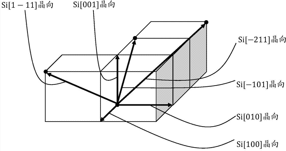
Fig. 1 is a schematic diagram of each crystal orientation of silicon involved in the present invention, and the present invention will be further described below in conjunction with Fig. 1 for different embodiments.

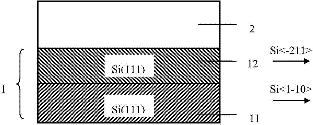
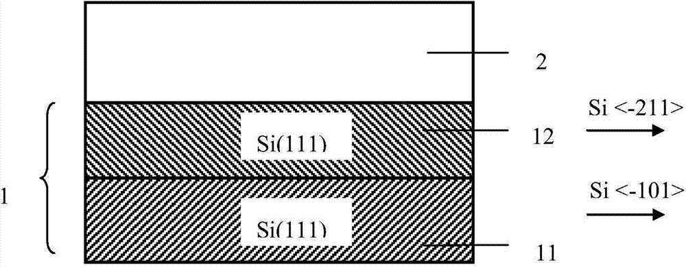
2 is a schematic structural diagram of a semiconductor substrate in the first embodiment of the present i...


PUM


Abstract

The invention discloses a semiconductor substrate, a semiconductor device and a semiconductor substrate manufacturing method. The semiconductor substrate comprises a first semiconductor layer and a second semiconductor layer which is arranged on the first semiconductor layer, wherein both the first semiconductor layer and the second semiconductor layer are respectively provided with a different dissociation surface in the vertical direction after symmetrically rotating along respective crystal lattice. The semiconductor substrate has a unique crystal lattice structure and a unique mechanical structure, the semiconductor substrate is set as a composite substrate structure, the harm of the stress applied to a semiconductor epitaxial layer on the semiconductor substrate can be reduced under the condition of the same substrate thickness, and the breaking probability of the semiconductor substrate can be reduced; meanwhile, the technological difficulty also can be alleviated, and the reliability of the semiconductor device can be enhanced.

Description

technical field The invention relates to the technical field of microelectronics, in particular to a semiconductor substrate, a semiconductor device and a semiconductor substrate manufacturing method. Background technique Group III nitrides represented by gallium nitride have attracted more and more attention, because group III nitrides can be widely used as light-emitting diodes (LEDs) for semiconductor lighting and high-power electronic devices. Due to the lack of intrinsic substrates, GaN devices are commonly fabricated on heterogeneous substrates, such as sapphire, silicon carbide, and silicon. Due to its wide applicability, silicon substrate has the best size and quality among the above-mentioned substrate materials. At present, the mainstream technology of complementary metal oxide semiconductor (CMOS) is based on 12-inch silicon substrate, and the price of silicon is unmatched by other materials. Therefore, preparing gallium nitride materials on large-scale silicon...

Claims


Application Information

Patent Timeline
IPC IPC(8): H01L33/00H01L33/20
CPCH01L33/0066H01L33/12H01L21/2007H01L21/187H01L21/0254H01L21/02609H01L33/00H01L33/0075H01L33/18H01L33/26
Inventor 程凯
Owner ENKRIS SEMICON
Why Eureka
Try Eureka