

DC offset cancellation circuit
A technology for eliminating circuit and DC offset, applied in the direction of DC level restoration device/bias distortion correction, baseband system components, etc. layout area, improve integration, eliminate the effect of DC offset
- Summary
- Abstract
- Description
- Claims
- Application Information
AI Technical Summary
Problems solved by technology
Method used
Image


Examples
Embodiment Construction
[0011] The present invention will be further described below in conjunction with the accompanying drawings and specific embodiments.
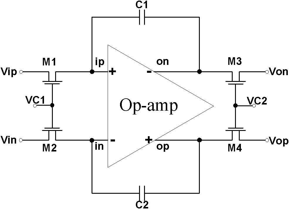
[0012] Such as figure 1 As shown, a DC offset elimination circuit includes a first transistor M1, a second transistor M2, a third transistor M3, a fourth transistor M4, a first feedback capacitor C1, a second feedback capacitor C2, a first voltage control signal port VC1, the second voltage control signal port VC2, the signal input positive terminal Vip, the signal input negative terminal Vin, the signal output positive terminal Vop, the signal output negative terminal Von and the operational amplifier Op-amp, wherein the drain of the first transistor M1 is connected to The signal input positive terminal Vip is connected, the source of the first transistor M1 is connected with the positive input terminal ip of the operational amplifier Op-amp; the drain of the second transistor M2 is connected with the signal input negative terminal Vin, and th...
PUM
 Abstract
Description
Claims
Application Information