Eureka AIR delivers breakthrough ideas for toughest innovation challenges, trusted by R&D personnel around the world.

Low-noise MEMS capacitive sensor interface circuit

A capacitive sensor and interface circuit technology, applied in the direction of logic circuit interface device, logic circuit connection/interface layout, amplifier using switched capacitors, etc., can solve the problem of signal-to-noise ratio reduction, gain accuracy deterioration, and overall power consumption increase of the interface circuit etc. to achieve the effect of reducing gain error, improving gain accuracy, and increasing circuit power consumption

Inactive Publication Date: 2022-06-21
西安水木芯邦半导体设计有限公司
View PDF0 Cites 0 Cited by
  • Summary
  • Abstract
  • Description
  • Claims
  • Application Information

AI Technical Summary

Problems solved by technology

However, the parasitic capacitance between the MEMS sensing element and the readout circuit causes two major problems: deterioration of gain accuracy and reduction of signal-to-noise ratio
However, the realization of low-noise performance usually leads to an increase in the overall power consumption of the interface circuit. Therefore, how to achieve low-noise performance of the interface circuit without increasing power consumption is a technical problem that needs to be solved urgently.

Method used


Image

  • Low-noise MEMS capacitive sensor interface circuit
  • Low-noise MEMS capacitive sensor interface circuit
  • Low-noise MEMS capacitive sensor interface circuit

Examples


Embodiment Construction

[0030] The specific embodiments of the present invention will be further described below with reference to the accompanying drawings.

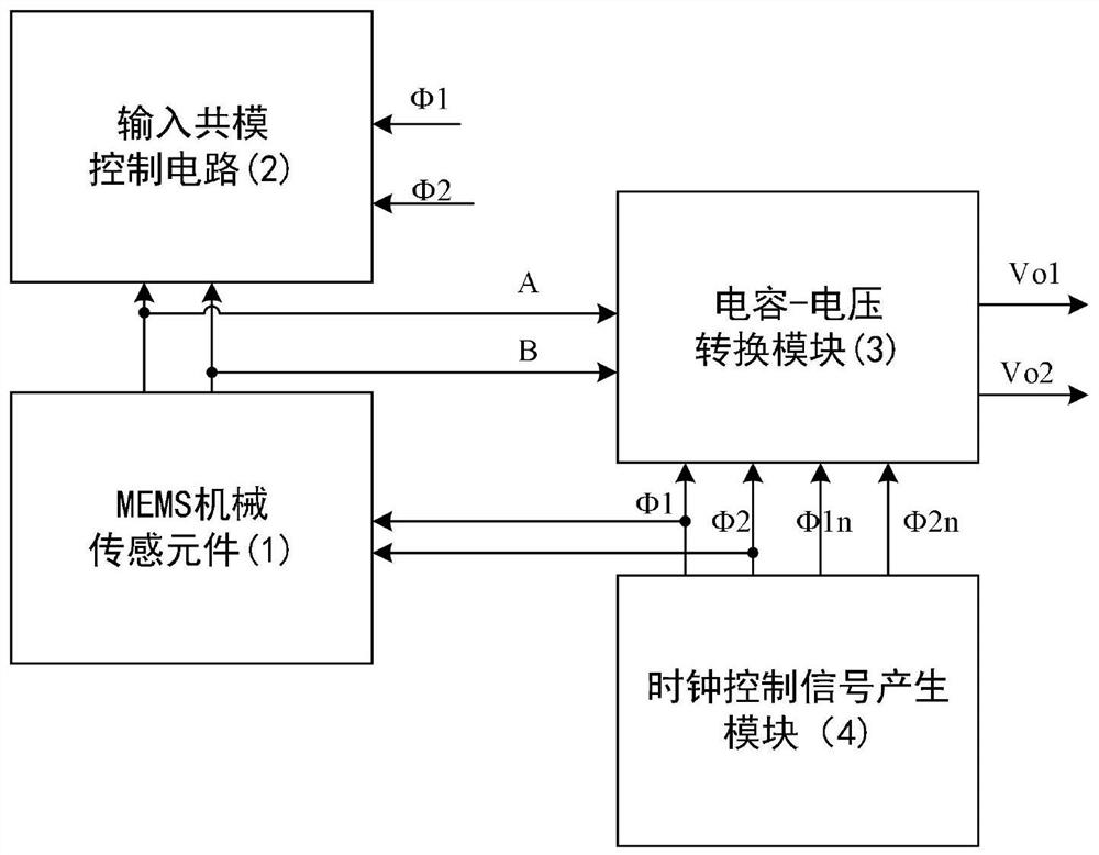
[0031] refer to figure 1 , the present invention includes a MEMS mechanical sensing element 1, an input common mode control circuit 2, a capacitance-voltage conversion module 3 and a clock control signal generation module 4;

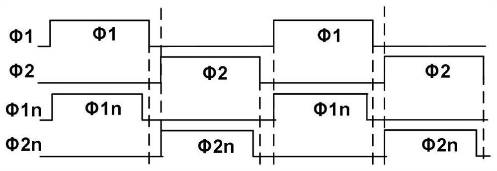
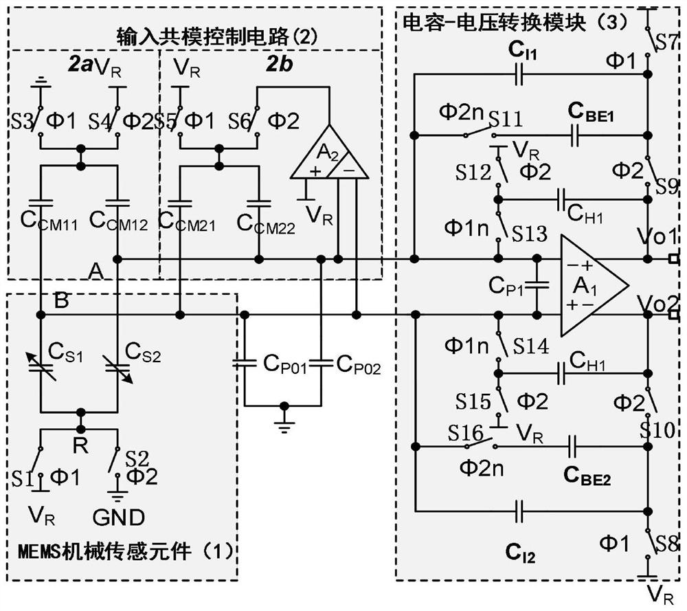
[0032] The MEMS mechanical sensing element 1 is used to convert the external acceleration signal into the variation of the MEMS mechanical capacitance. The MEMS mechanical sensing element 1 is driven by the clock control signals Φ1 and Φ2 generated by the clock control signal generating module 4 to generate sensor charges. Signals A and B, the sensor charge signals A and B both include common mode charge components and differential mode charge components, wherein the common mode charge components are absorbed by the input common mode control circuit 2, and the differential mode components are transmitted to the capacitor...


PUM


Abstract

The invention discloses a low-noise MEMS capacitive sensor interface circuit which mainly solves the problems of gain errors and circuit noise deterioration. The device comprises an MEMS mechanical sensing element, an input common-mode control circuit, a capacitance-voltage conversion module and a clock control signal generation module. The MEMS mechanical sensing element is used for converting an external acceleration signal into a variable quantity of an MEMS mechanical capacitor and generating sensor charge signals A and B; the input common-mode control circuit is used for absorbing common-mode components of sensor charge signals, and other differential-mode components are transmitted to the integrating capacitor for signal amplification, so that conversion of capacitor voltage is realized. And the gain precision is improved by introducing the sampling holding capacitor, so that the original high-gain operational amplifier can be replaced by the low-gain operational amplifier. Due to the introduction of the bandwidth compensation capacitor, the interface circuit can work under a clock with higher frequency, and the noise floor of the interface circuit is reduced. The purposes of not additionally increasing the power consumption of the circuit and reducing the noise of the interface circuit are achieved.

Description

technical field [0001] The present invention belongs to the field of integrated circuits, and more particularly relates to the processing of signals of microelectromechanical systems (MEMS) sensors. Background technique [0002] MEMS, or Micro-Electro-Mechanical System, is a multidisciplinary frontier research field developed on the basis of microelectronics technology. After more than 40 years of development, it has become one of the major scientific and technological fields that the world pays attention to. MEMS sensors are becoming more and more popular due to their small size. MEMS sensor is a new type of sensor manufactured using microelectronics and micromachining technology. Compared with traditional sensors, it has the characteristics of small size, light weight, low cost, low power consumption, high reliability, suitable for mass production, easy integration and realization of intelligence. [0003] MEMS capacitive sensors play an important role in a wide range o...

Claims


Application Information

Patent Timeline
Patent Type & Authority Applications(China)
IPC IPC(8): H03F3/00H03F1/42H03F1/08H03F1/26H03K19/003H03K19/0175G01D5/24
CPCH03F3/005H03F1/42H03F1/08H03F1/26H03K19/00346H03K19/017509G01D5/24
Inventor 来新泉王宇恒袁昕李继生李文岑
Owner 西安水木芯邦半导体设计有限公司
Why Eureka
Eureka Blog
Learn More