Method for preparing gold-phase section samples aiming at embedded printed-circuit board
A printed circuit board and metallographic sectioning technology, which is applied in the preparation of test samples and sampling devices, can solve the problems of deformation, excessive grinding, and bending of sliced samples, so as to reduce testing costs, ensure stability and Consistency, the effect of improving detection efficiency
- Summary
- Abstract
- Description
- Claims
- Application Information
AI Technical Summary
Problems solved by technology
Method used
Image

Examples
Embodiment Construction
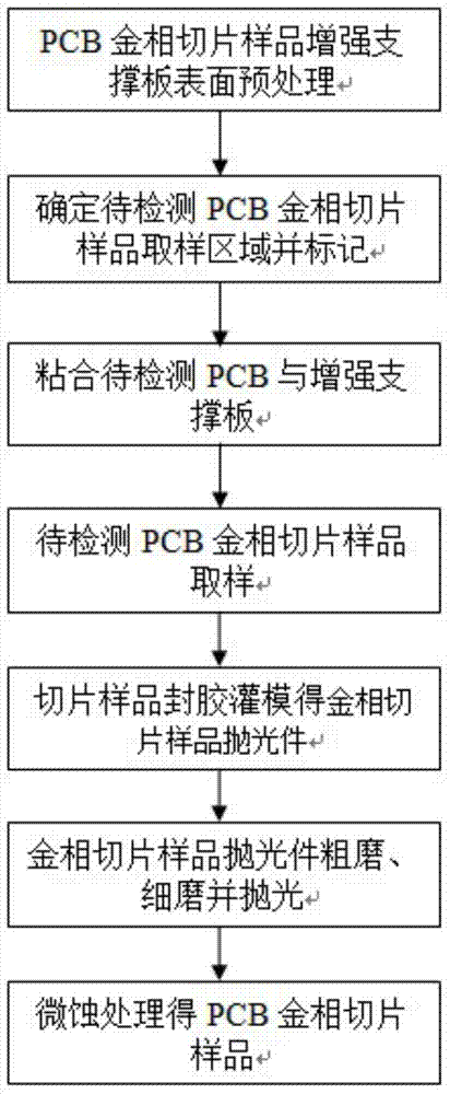
[0024] The present invention will be described in further detail below in conjunction with specific embodiments and accompanying drawings.
[0025] A method for preparing a metallographic section sample of a 4-layer embedded capacitor printed circuit board, comprising the steps of:
[0026] Step 1. Select a piece of FR-4 substrate material with a thickness of 3mm, and cut it into a metallographic slice reinforced support plate of 5×5cm; first, roughen the surface of the FR-4 substrate with P120 sandpaper, and then put it into the cleaning solution for cleaning , and then cleaned with deionized water, and finally dried in an oven at 120°C for 30 minutes;
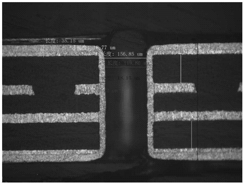
[0027] Step 2. Take the 4-layer embedded capacitor PCB board to be tested, cut it into a 5×5cm shape with scissors, determine the sampling area to be tested and mark it;
[0028] Step 3. Place the roughened and clean FR-4 substrate material reinforced support plate on the horizontal platform, and evenly coat a layer of α-cya...
PUM
| Property | Measurement | Unit |
|---|---|---|
| Thickness | aaaaa | aaaaa |
Abstract
Description
Claims
Application Information
 - Generate Ideas
- Intellectual Property
- Life Sciences
- Materials
- Tech Scout
- Unparalleled Data Quality
- Higher Quality Content
- 60% Fewer Hallucinations
Browse by: Latest US Patents, China's latest patents, Technical Efficacy Thesaurus, Application Domain, Technology Topic, Popular Technical Reports.
© 2025 PatSnap. All rights reserved.Legal|Privacy policy|Modern Slavery Act Transparency Statement|Sitemap|About US| Contact US: help@patsnap.com