Pixel driving circuit, array substrate, display device and pixel driving method

A pixel drive circuit and drive unit technology, applied in static indicators, instruments, etc., can solve problems such as changes in OLED luminance, sensitivity to changes in operating current, uneven luminance of display devices, etc., to achieve uniform luminance, improve The effect of uniformity

Active Publication Date: 2014-04-02
HEFEI BOE OPTOELECTRONICS TECH +1
View PDF6 Cites 28 Cited by
  • Summary
  • Abstract
  • Description
  • Claims
  • Application Information

AI Technical Summary

Problems solved by technology

[0004] In the AMOLED pixel drive circuit provided by the prior art, the threshold voltage of T1 will vary with the deviation of the process. After T1 is turned on, the working current of OLED is related to the threshold voltage of T1, and the luminous brightness of OLED is related to the working current. is quite sensitive to changes, so changes in the threshold voltage of T1 will cause considerable changes in the luminance of OLEDs
The threshold voltage will change due to process fluctuations or changes in the temperature of the display device during operation, which will lead to uneven luminance of the display device.

Method used


Image

  • Pixel driving circuit, array substrate, display device and pixel driving method
  • Pixel driving circuit, array substrate, display device and pixel driving method
  • Pixel driving circuit, array substrate, display device and pixel driving method

Examples


Embodiment Construction

[0042] In order for those skilled in the art to better understand the technical solution of the present invention, the pixel driving circuit, array substrate, display device and pixel driving method provided by the present invention will be described in detail below with reference to the accompanying drawings.

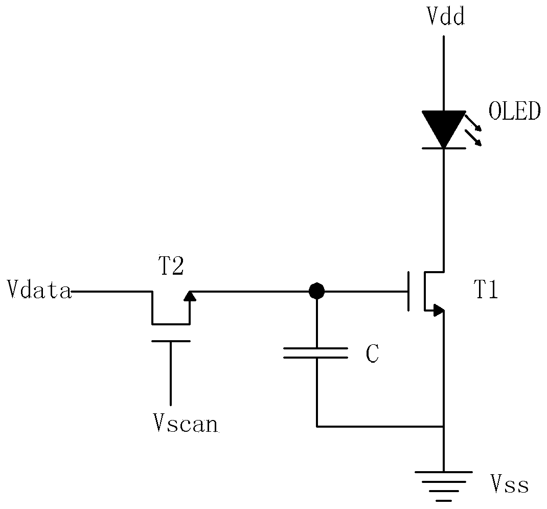
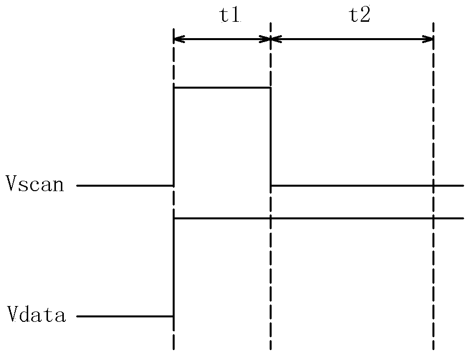
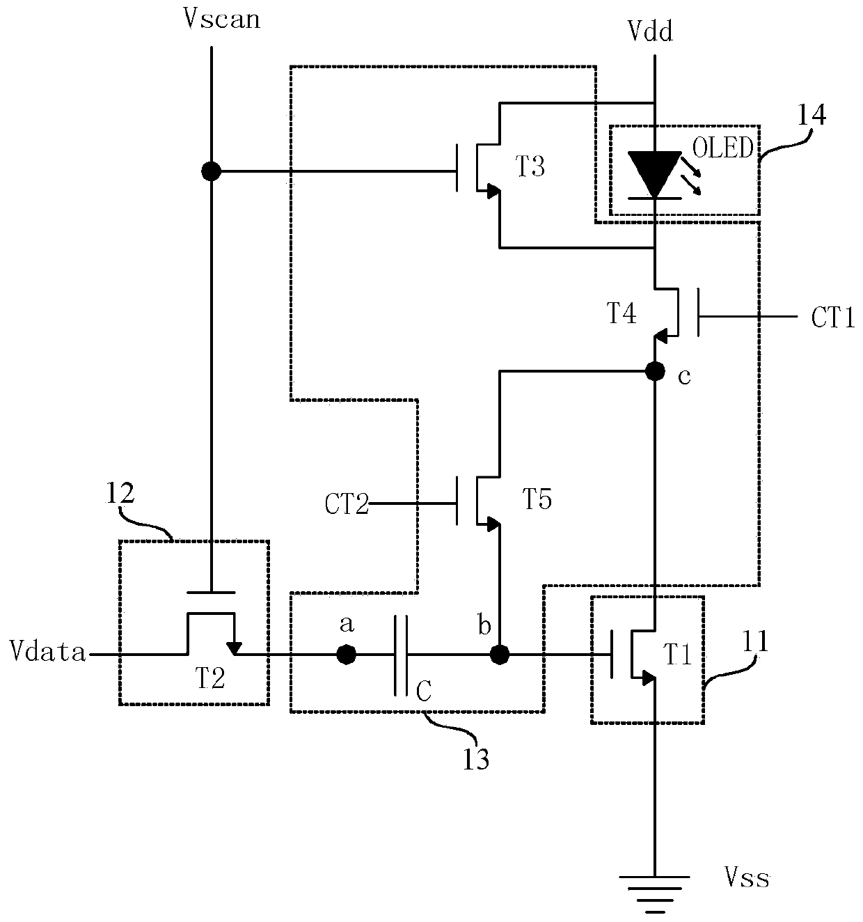
[0043] image 3 A schematic structural diagram of a pixel driving circuit provided in Embodiment 1 of the present invention, as shown in image 3 As shown, the pixel driving circuit includes: a driving unit 11, a switching unit 12, a threshold voltage compensation module 13, and a light emitting device 14. The threshold voltage compensation module 13 is respectively connected to the scanning signal line, the first control line CT1, the second control line CT2, The second power supply is connected to the switch unit 12, the light emitting device 14 is connected to the second power supply and the threshold voltage compensation module 13 respectively, the drive unit 11 is...


PUM


Abstract

The invention discloses a pixel driving circuit, an array substrate, a display device and a pixel driving method. The pixel driving circuit can comprise a driving unit, a switch unit, a threshold voltage compensation module and a luminescent device, wherein the threshold voltage compensation module is respectively connected with a scanning signal wire, a first control wire, a second control wire, a second power supply and a switch unit, the luminescent device is respectively connected with a second power supply and the threshold voltage compensation module, the driving unit is respectively connected with a first power supply and the threshold voltage compensation module, the switch unit is respectively connected with the scanning signal wire and a data signal wire, and the threshold voltage compensation module comprises a threshold voltage maintaining unit, an anti-interference unit, an auxiliary gating unit and a charge and discharge control switch unit. The work current of the luminescent device is irrelevant to the threshold voltage of the driving unit, so the luminescent brightness of the luminescent device is uniform, and further, the luminescent brightness uniformity of the display device is improved.

Description

technical field [0001] The present invention relates to the field of display technology, in particular to a pixel driving circuit, an array substrate, a display device and a pixel driving method. Background technique [0002] With the advancement of display technology, more and more Active Matrix Organic Light Emitting Diode (AMOLED) display devices have entered the market. Compared with traditional thin film transistor liquid crystal display devices (Thin Film Transistor Liquid Crystal Display, referred to as: TFT LCD), AMOLED display device has faster response speed, higher contrast ratio and wider viewing angle, so AMOLED display device has been valued by more and more panel manufacturers. [0003] figure 1 It is a schematic structural diagram of an AMOLED pixel driving circuit in the prior art, such as figure 1 As shown, the pixel driving circuit includes a first thin film transistor (Thin Film Transistor, TFT for short) T1, a second thin film transistor T2, a capacito...

Claims


Application Information

Patent Timeline
Patent Type & Authority Applications(China)
IPC IPC(8): G09G3/32
CPCG09G2300/0861G09G2320/043G09G2300/0819G09G2310/0262G09G3/3233G09G2300/0842G09G3/3258G09G3/3291G09G2300/0809G09G2310/0202G09G2320/0233G09G2320/0646
Inventor 胡祖权公伟刚
Owner HEFEI BOE OPTOELECTRONICS TECH
Why Eureka
Try Eureka