Liquid crystal lens, manufacturing method of liquid crystal lens and display device

A technology of a liquid crystal lens and a manufacturing method, which can be applied in nonlinear optics, instruments, optics, etc., can solve the problems of uneven refractive index change, reducing the refractive effect of liquid crystal lens, etc.

Active Publication Date: 2014-04-09
BOE TECH GRP CO LTD
4 Cites 7 Cited by

AI-Extracted Technical Summary

Problems solved by technology

[0004] like figure 2 As shown, in the liquid crystal lens element with oblique electrodes, there is a large lateral electric field near the electrode, where the liquid crystal pretilt direction conflict...

Method used

A kind of liquid crystal lens manufacturing method that the embodiment of the present invention provides, by forming flat layer between the first transparent electrode layer and the first liquid crystal alignment layer, the first liquid crystal alignment layer is moved to the position with weaker lateral electric field , thereby reducing the liquid crystal phase error and improving the refraction effect of the liquid crystal lens.
In the existing liquid crystal lens as shown in Figure 1, the first substrate 1 and the second substrate 2 form a larger voltage difference, and two adjacent transparent electrodes in the first transparent electrode layer 5 form a smaller voltage difference respectively, A lateral electric field is formed between two adjacent transparent electrodes, and the liquid crystal alignment direction of the first liquid crystal alignment layer 4 is not parallel to the direction of the lateral electric field, resulting in liquid crystal phase mismatch (see FIG. 2 ). In this embodiment, on the basis of the above-mentioned liquid crystal lens, a flat layer 6 is formed in the first transparent electrode layer 5 and the first liquid crystal alignment layer 4, and the first liquid crystal alignment layer 4 is moved to the lateral direction through the flat layer 6. The position where the electric field is weaker, thereby reducing the phase error of the liquid crystal.
In this embodiment, the thickness of the flat layer added between the transparent electrode layer and the first liquid crystal alignment layer is 1 μm to 5 μm, so that under the premise that the technical effect is guaranteed...

Abstract

The invention provides a liquid crystal lens, a manufacturing method of the liquid crystal lens, and a display device, and belongs to the technical field of display. The liquid crystal lens comprises a first substrate, a second substrate, a liquid crystal layer, a first transparent electrode layer, a first liquid crystal alignment layer, a second transparent electrode layer and a second liquid crystal alignment layer, wherein the liquid crystal layer is located between the first substrate and the second substrate, the first transparent electrode layer and the first liquid crystal alignment layer are located on the first substrate and are close to one side of the liquid crystal layer, and the second transparent electrode layer and the second liquid crystal alignment layer are located at the portion, close to one side of the liquid crystal layer, of the second substrate. The liquid crystal lens further comprises a flat layer arranged between the first transparent electrode layer and the first liquid crystal alignment layer. According to the liquid crystal lens, the flat layer is formed between the first transparent electrode layer and the first liquid crystal alignment layer, and the first liquid crystal alignment layer moves the position with the weaker lateral electric field, so that liquid crystal dislocation is reduced, and the refraction effect of the liquid crystal lens is improved.

Application Domain

Non-linear optics

Technology Topic

DislocationElectric field +5

Image

  • Liquid crystal lens, manufacturing method of liquid crystal lens and display device
  • Liquid crystal lens, manufacturing method of liquid crystal lens and display device
  • Liquid crystal lens, manufacturing method of liquid crystal lens and display device

Examples

  • Experimental program(3)

Example Embodiment

[0032] Example 1:
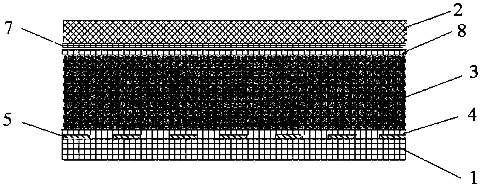
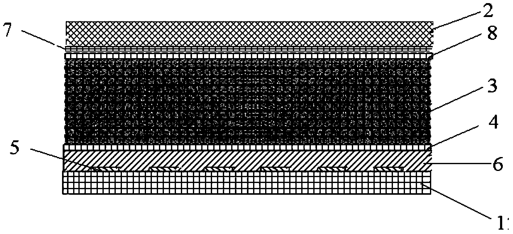
[0033] In order to solve the above-mentioned technical problems, embodiments of the present invention provide a liquid crystal lens, such as image 3 Shown is a schematic diagram of the structure of a liquid crystal lens provided by an embodiment of the present invention. The liquid crystal lens includes: a first substrate 1, a second substrate 2, a liquid crystal layer 3 between the first substrate 1 and the second substrate 2, and The first transparent electrode layer 5 and the first liquid crystal alignment layer 4 on the side of the first substrate 1 close to the liquid crystal layer 3 and between the first transparent electrode layer 5 and the first liquid crystal alignment layer 4 The flat layer6. A second transparent electrode layer 7 is provided on the side of the second substrate 2 close to the liquid crystal layer 3. The second transparent electrode layer 7 is a full-surface electrode, and there is also a second transparent electrode layer 7 and the liquid crystal layer 3. There is a second liquid crystal alignment layer 8.
[0034] Wherein, the first substrate 1 and the second substrate 2 are both glass substrates. The first transparent electrode layer 5 includes a plurality of transparent electrodes arranged at intervals, and the transparent electrodes are strip-shaped electrodes. Such as figure 1 As shown in the liquid crystal lens, when the liquid crystal lens is in operation, the liquid crystal layer 3 deflects the liquid crystal molecules under the action of the upper and lower electric fields. At the same time, there is a voltage gap between the two adjacent transparent electrodes of the first transparent electrode 5, and a lateral electric field is formed between the two adjacent transparent electrodes, causing the liquid crystal molecules to deflect laterally. However, in this embodiment, due to the proximity The liquid crystal molecules near the first transparent electrode layer 5 are separated by the added flat layer 6 and are located in a weak electric field. Therefore, the liquid crystal molecules undergo lateral deflection opposite to the pretilt angle direction to reduce the phenomenon of dislocation, thereby improving the liquid crystal The refraction effect of the lens. Such as Figure 4 Shown is a graph of refractive index changes in the horizontal profile of a liquid crystal lens provided by an embodiment of the present invention, which is represented by Figure 4 It can be seen that due to the reduction of the phase misalignment of the liquid crystal, the refractive index of the liquid crystal changes more continuously.
[0035] Such as figure 1 In the conventional liquid crystal lens shown, the first substrate 1 and the second substrate 2 form a large voltage difference, two adjacent transparent electrodes in the first transparent electrode layer 5 respectively form a small voltage difference, and two adjacent transparent electrodes A lateral electric field is formed between the first liquid crystal alignment layer 4 and the liquid crystal orientation direction of the first liquid crystal alignment layer 4 is not parallel to the direction of the lateral electric field, resulting in a liquid crystal phase shift (see figure 2 ). In this embodiment, on the basis of the above-mentioned liquid crystal lens, a flat layer 6 is formed in the first transparent electrode layer 5 and the first liquid crystal alignment layer 4, and the first liquid crystal alignment layer 4 is moved to the lateral direction through the flat layer 6 The position where the electric field is weaker reduces the phase shift of the liquid crystal.
[0036] In the liquid crystal lens provided by the embodiment of the present invention, the plurality of spaced transparent electrodes of the first transparent electrode layer 5 are separated by a flat layer of transparent insulating material.
[0037] The flat layer 6 is made of a transparent insulating resin material that transmits light and is convenient for coating and processing. The present invention defines the material of the flat layer 6 and forms the flat layer 6 with a transparent insulating resin material so that the added flat layer 6 The initial function of the liquid crystal lens is not affected. The transparent insulating resin material used in the flat layer includes light-curing transparent resin photoresist, or thermosetting acrylic-based resin.
[0038] The thickness of the flat layer is 1 μm to 5 μm, and the flat layer within this thickness range makes the increase in the thickness of the liquid crystal lens insignificant under the premise of ensuring the technical effect, and will not affect the user experience.

Example Embodiment

[0039] Example 2:
[0040] The embodiment of the present invention also provides a method for manufacturing a liquid crystal lens, such as Figure 5 Shown is a flowchart of a method for manufacturing a liquid crystal lens provided by an embodiment of the present invention, and the method includes:
[0041] 201: sequentially forming a pattern including a first transparent electrode layer, a flat layer, and a first liquid crystal alignment layer on a first substrate;
[0042] In the embodiment of the present invention, a patterning process is used to sequentially form a pattern including a transparent electrode layer, a flat layer, and a first liquid crystal alignment layer on the first substrate; wherein the patterning process includes patterning processes such as exposure, development, and etching, or printing and Composition techniques such as grid printing.
[0043] Wherein, the step of forming the flat layer includes: forming the flat layer by spin coating, deposition or printing.
[0044] Among them, the flat layer is preferably a transparent and insulating resin material, so that the added flat layer does not affect the initial effect of the liquid crystal lens.
[0045] In this embodiment, the thickness of the flat layer added between the transparent electrode layer and the first liquid crystal alignment layer is 1 μm to 5 μm, so that under the premise of ensuring the technical effect, the increase in the thickness of the liquid crystal lens is not significant and will not affect the user's Experience.
[0046] 202: Align with a pre-made second substrate provided with a second transparent electrode layer and a second liquid crystal alignment layer and inject liquid crystals to form the liquid crystal lens.
[0047] The manufacturing method of the second substrate is the same as that of the first substrate. After step 201 is completed, the second substrate provided with the second transparent electrode layer and the second liquid crystal alignment layer is aligned with the first substrate after step 201 is completed. After the cell is aligned, liquid crystal is injected between the first liquid crystal alignment layer and the second liquid crystal alignment layer to form a liquid crystal lens.
[0048] An embodiment of the present invention provides a method for manufacturing a liquid crystal lens. By forming a flat layer between the first transparent electrode layer and the first liquid crystal alignment layer, the first liquid crystal alignment layer is moved to a position where the lateral electric field is weaker, thereby reducing The phase shift of the liquid crystal is improved, and the refraction effect of the liquid crystal lens is improved.

Example Embodiment

[0049] Example 3:
[0050] An embodiment of the present invention also provides a display device, including the liquid crystal lens described in the first embodiment. The display device includes, but is not limited to, a three-dimensional display.

PUM

PropertyMeasurementUnit
Thickness1.0 ~ 5.0µm

Description & Claims & Application Information

We can also present the details of the Description, Claims and Application information to help users get a comprehensive understanding of the technical details of the patent, such as background art, summary of invention, brief description of drawings, description of embodiments, and other original content. On the other hand, users can also determine the specific scope of protection of the technology through the list of claims; as well as understand the changes in the life cycle of the technology with the presentation of the patent timeline. Login to view more.
Why Eureka
Try Eureka