Method for manufacturing circuit board

A manufacturing method and circuit board technology, applied in the directions of printed circuit manufacturing, printed circuits, electrical components, etc., can solve the problems of poor bonding force of heat dissipation conductors 4, affecting the welding effect of heating components, and uncertainty of the height of prepreg 3, etc. The effect of sunken or convex problems

Active Publication Date: 2014-04-09
GCI SCI & TECH
View PDF4 Cites 1 Cited by
  • Summary
  • Abstract
  • Description
  • Claims
  • Application Information

AI Technical Summary

Problems solved by technology

[0005] But, there is following shortcoming in the circuit board that above-mentioned method makes: the radiating conductor 4 that embeds is fixed in the through groove completely by the thermal curing of the resin flow glue of prepreg 3, and resin flow glue does not pass through high-pressure curing process, makes embedding The heat dissipation conductor 4 has poor bonding force; the height difference between the em

Method used


Image

  • Method for manufacturing circuit board
  • Method for manufacturing circuit board
  • Method for manufacturing circuit board

Examples


Example Embodiment

[0025] The technical solutions in the embodiments of the present invention will be clearly and completely described below in conjunction with the accompanying drawings in the embodiments of the present invention. Obviously, the described embodiments are only a part of the embodiments of the present invention, rather than all the embodiments. Based on the embodiments of the present invention, all other embodiments obtained by those of ordinary skill in the art without creative work shall fall within the protection scope of the present invention.

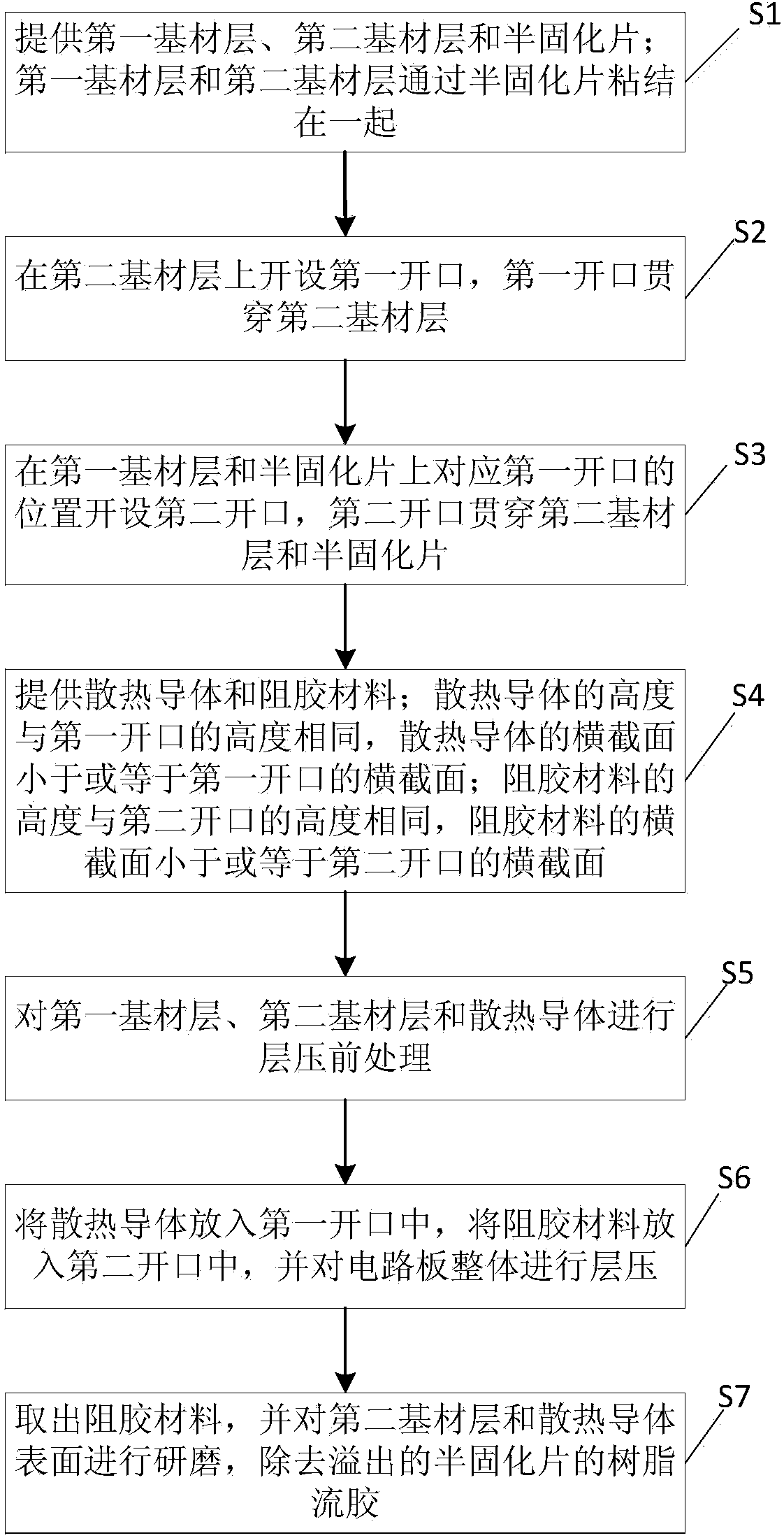
[0026] See figure 1 , Is a schematic flow chart of an embodiment of a method for manufacturing a circuit board provided by the present invention. The method specifically includes the following steps:

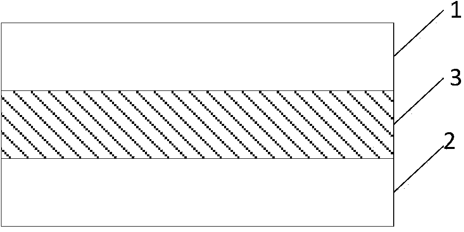
[0027] S1, providing a first substrate layer, a second substrate layer and a prepreg; the first substrate layer and the second substrate layer are bonded together by the prepreg;

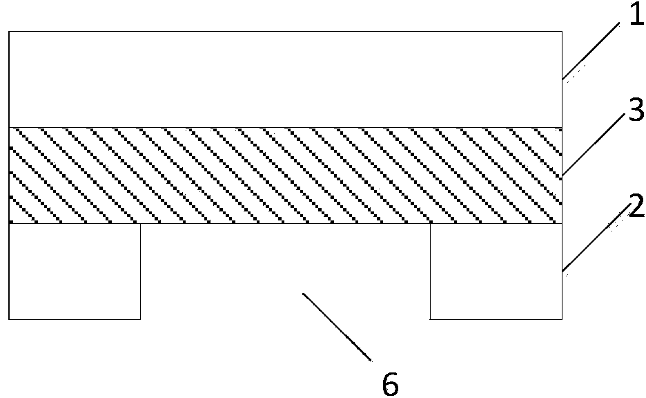
[0028] S2, a first opening is opened on the second substrate ...


PUM


Abstract

The invention discloses a method for manufacturing a circuit board. The method includes the steps that S1, a first base material layer and a second base material layer are bonded together through a prepreg; S2, a first opening is formed in the second base material layer, and the first opening penetrates through the second base material layer; S3, second openings, corresponding to the first opening in position, are formed in the first base material layer and the prepreg, and the second openings penetrate through the first base material layer and the prepreg; S4, a radiating conductor and glue blocking materials are provided; S5, laminating pretreatment is carried out on the first base material layer, the second base material layer and the radiating conductor; S6, the radiating conductor is placed into the first opening, the glue blocking materials are placed into the second openings, and lamination is conducted on the entire circuit board; S7, the glue blocking materials are taken out, and the surface of the second base material layer and the surface of the radiating conductor are ground. By means of the method for manufacturing the circuit board, the radiating problem of the circuit board can be solved, the manufacturing method of the circuit board is simple, and the embedded effect of the radiating conductor is good.

Description

Technical field [0001] The invention relates to the technical field of circuit board manufacturing technology, in particular to a manufacturing method of a circuit board. Background technique [0002] With the development of the electronics industry, the volume of electronic products is getting smaller and smaller, and the power density is getting higher and higher. How to find the best method for circuit board heat dissipation and structural design has become a huge challenge in today's electronics industry design. At present, the commonly used circuit board heat dissipation methods include two methods: using a metal substrate to make a circuit board and welding a metal substrate on the circuit board. However, these two processes have the disadvantages of large consumption of metal materials, complex manufacturing processes, high costs, and bulky volume. Especially for some products with relatively low heat dissipation power requirements, higher processing costs and complex proc...

Claims


Application Information

Patent Timeline
IPC IPC(8): H05K3/00
Inventor 黄德业陈亮唐有军杨泽华任代学
Owner GCI SCI & TECH
Why Eureka
Try Eureka