Visual detection equipment of circuit board

A visual inspection and circuit board technology, applied in the direction of electrical components, electrical components, optical testing defects/defects, etc., can solve the problems of inaccurate detection, slow detection speed, low detection efficiency, etc., to achieve cost saving, accurate detection, and detection The effect of large coverage

Inactive Publication Date: 2014-04-16
GUANGDONG LYRIC ROBOT INTELLIGENT AUTOMATION CO LTD
9 Cites 58 Cited by

AI-Extracted Technical Summary

Problems solved by technology

[0002] In the prior art, after soldering and packaging the various components of the circuit board, it is necessary to carry out some defect detection on the circuit board to ensure that the output circuit board is a finished product, so as to complete the installation or follow-up of the circuit board for the post station. Therefore, the inspection of the circuit board ...

Abstract

The invention discloses visual detection equipment of a circuit board. The visual detection equipment of the circuit board comprises a bearing plate and a control system, a conveyor trough arranged on the bearing plate, a conveyor belt clamped in the conveyor trough and used for conveying a supplied to-be-detected circuit board, a first visual detection device, a second visual detection device, a finished product collection device and a defective product collection device, wherein the first visual detection device comprises a first CCD (charge coupled device) imaging system and a first blocking mechanism; the second visual detection device comprises a second CCD imaging system and a second blocking mechanism; the finished product collection device is used for collecting finished circuit boards after detection; and the defective product collection device comprises a defective product rejecting manipulator and a defective product collection conveyor belt used for collecting defective products. Compared with the prior art, only one conveyor belt is adopted for the detection process, so that the cost is saved greatly, and the visual detection equipment of the circuit board can perform detection on a first surface and a second surface of the circuit board respectively, the detection covering range is large, and the detection speed is high.

Application Domain

Technology Topic

Image

  • Visual detection equipment of circuit board

Examples

  • Experimental program(1)

Example Embodiment

[0023] The technical solution of the present invention will be described in detail below with reference to the drawings and specific embodiments, so as to understand the essence of the present invention more clearly and intuitively.
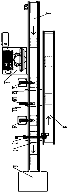
[0024] Such as figure 1 As shown, a circuit board visual inspection equipment provided by the present invention includes a carrier board and a control system, and it also includes:
[0025] Conveying trough, the conveying trough is provided on the carrying plate;
[0026] Conveyor belt 1, the conveyor belt 1 is clamped in the conveying trough for conveying incoming circuit boards to be tested;
[0027] It should be emphasized that, in the present invention, the transportation of incoming materials from the circuit board to be inspected, the inspection of the circuit board, and the output of the finished circuit board that have passed the inspection are all conveyed by a conveyor belt 1, that is, the present invention is compared with the prior art , For the inspection process, only one conveyor belt 1 is used, that is, the linear conveyor is used to connect the stations. Compared with the traditional conveyor belt, the conveyor belt, the inspection conveyor belt, the output conveyor belt, etc., it greatly saves costs and avoids resources. Waste.
[0028] In this embodiment, the circuit board visual inspection equipment of the present invention further includes:
[0029] The first visual inspection device includes a first CCD imaging system 2 and a first blocking mechanism 3; the first CCD imaging system 2 is located above the conveyor belt 1, and its function is to detect Test the first side of the circuit board; the first blocking mechanism 3 is located at the right end of the first CCD imaging system 2 and is signaled to the first CCD imaging system 2; when the first CCD imaging system 2 detects The circuit board to be tested has a defect, that is, when the detected circuit board is unqualified, the first blocking mechanism 3 will block the unqualified circuit board; when the tested circuit board is qualified, the first blocking mechanism The mechanism 3 will not block the qualified circuit boards, so the qualified circuit board products are then conveyed to the rear product collection device 6 along the driving direction of the conveyor belt 1.
[0030] A second visual inspection device, the second visual inspection device includes a second CCD imaging system 4 and a second blocking mechanism 5, the second CCD imaging system 4 is provided at the right end of the first blocking mechanism 3, located at the The upper part of the conveyor belt 1 is used to detect the second surface of the circuit board to be tested; the second blocking mechanism 5 is located at the right end of the second CCD imaging system 4, and is signal connected to the second CCD imaging system 4 ; Similarly, when the second CCD imaging system 4 detects a defect in the circuit board to be tested, that is, when the detected circuit board is unqualified, the second blocking mechanism 5 will perform the inspection on the unqualified circuit board Block; when the detected circuit board is qualified, the second blocking mechanism 5 will not block the qualified circuit board, so that the qualified circuit board products are then transported along the conveyor belt to the rear product collection device 6 .
[0031] The product collection device 6 in this embodiment is located at the right end of the conveyor belt 1 and is connected to the conveyor belt 1, and its function is to collect the qualified circuit board products after testing;
[0032] A defective product collection device, the defective product collection device includes a defective product rejection robot 7 and a defective product collection conveyor belt 8, the defective product collection conveyor belt 8 is located behind the conveyor belt 1; the defective product rejection robot 7 is located at Between the second CCD imaging system 4 and the second blocking mechanism 5 and above the conveyor belt 1; when the first CCD imaging system 2 and/or the second CCD imaging system 4 detects When the test circuit board is unqualified, the defective product rejection manipulator 7 sucks the unqualified circuit board to the defective product collection conveyor belt 8.
[0033] The present invention also includes a display terminal 9, which is located in front of the carrier board and is signal-connected to the control system for setting detection content and displaying the first CCD imaging system 2 and the second CCD imaging system. System 4 detects the detection information of the circuit board to be tested.
[0034] Preferably, the present invention also includes a multi-axis manipulator 10 for turning the circuit board and a third blocking mechanism 11, and the multi-axis manipulator 10 is located between the first blocking mechanism 3 and the second CCD. Between the imaging systems 4 and above the conveyor belt 1, the third blocking mechanism 11 is located between the multi-axis manipulator 10 and the second CCD imaging system 4; when it is necessary to simultaneously detect the first circuit board under test On one side and the second side, when the circuit board detected by the first CCD imaging system 2 is qualified, the qualified circuit board is conveyed by the conveyor belt 1 to the third blocking mechanism 11, and the third blocking mechanism 11 When the sensor connected to the mechanism 11 senses the qualified circuit board, the third blocking mechanism 11 blocks the qualified circuit board immediately and transmits the signal to the multi-axis manipulator 10, and the multi-axis The manipulator 10 immediately turns over the qualified circuit board. At the same time, after the multi-axis manipulator 10 adjusts the position of the qualified circuit board, the third blocking mechanism 11 automatically rises to execute the circuit board. After being turned over, the qualified circuit board is then transported along the transmission direction of the conveyor belt 1 to wait for the second CCD imaging system 4 to complete the inspection of the second side of the qualified circuit board.
[0035] Further, the defective product rejection manipulator 7 is a suction cup manipulator.
[0036] Moreover, the working voltage of the circuit board visual inspection equipment of the present invention is AC210V-AC230V, and the working pressure is 0.5MPa-1.0MPa.
[0037] To facilitate a better understanding of the working principle of the present invention, figure 1 As shown, the specific implementation of the present invention is as follows: First, the customer confirms the content to be tested, that is, according to the customer’s needs, the customer proposes to detect a particular circuit node or a certain electronic component in the circuit board, etc. The content of the test is set as the test point. After the content to be tested is determined, the operator will bundle the wiring on the circuit board to be tested, and after fixing it, it can be placed on the conveyor belt 1 for positioning and power on Switch, the conveyor belt 1 immediately drives, transports the circuit board to be tested to the lower end of the first CCD imaging system 2, turns on the first CCD camera of the first CCD imaging system 2, and adjusts the lens position of the first CCD camera through the control system. Make it correspond to the position of the detection point in the circuit board to be detected, the first CCD camera will detect the detection point of the circuit board to be detected, and through photoelectric conversion, the optical signal is converted into a video signal and transmitted to the display Terminal 9 to facilitate real-time inspection information for operators;
[0038] When the second side of the circuit board needs to be detected, the second CCD imaging system 4 can be turned on, and when the second side of the circuit board does not need to be detected, the second CCD imaging system 4 does not need to be turned on. The detection principle of the second CCD imaging system 4 on the circuit board is the same as the detection principle of the first CCD imaging system 2 on the circuit board, that is, according to customer needs, if the customer needs to detect a certain solder joint on the second side of the circuit board, The solder joint is set as a detection point, and the second CCD imaging system 4 detects the light signal and converts the light signal into a video signal and transmits it to the display terminal 9, so that the operator can check the detection information in real time;
[0039] When the circuit board detected by the first CCD imaging system 2 has a defect, because the first blocking mechanism 3 is in signal connection with the first CCD imaging system 2, the first CCD imaging system 2 will detect the defect The signal is sent to the first blocking mechanism 3. After receiving the signal, the first blocking mechanism 3 will block the defective circuit board. At the same time, the first blocking mechanism 3 transmits the signal To the defective product rejection manipulator 7, the defective product rejection manipulator 7 picks up the defective circuit board, and transfers the defective circuit board to the defective product collection conveyor belt 8, and the defective product collection conveyor belt 8 Collect and transfer defective circuit boards; similarly, when the circuit board detected by the second CCD imaging system 4 is defective, the signals from the second blocking mechanism 5 and the second CCD imaging system 4 Connected, the second CCD imaging system 4 sends a defect signal during detection to the second blocking mechanism 5, and after receiving the signal, the second blocking mechanism 5 will block the defective circuit board. At the same time, the second blocking mechanism 5 transmits the signal to the defective product rejection manipulator 7, and the defective product rejection manipulator 7 sucks the defective circuit board and transfers the defective circuit board to the non-defective circuit board. The good product collection conveyor belt 8 collects and transfers defective circuit boards by the defective product collection conveyor belt 8.
[0040] It should be noted that when the customer needs to detect both the first side and the second side of the circuit board to be inspected, the first CCD imaging system 2 is used for inspection, and the circuit board that fails the inspection is rejected by the defective product removal manipulator. 7 Suction the unqualified circuit board to the defective product collection conveyor belt 8, inspect the qualified circuit board, and turn the circuit board over by the multi-axis manipulator 10 to turn it over to the second side of the circuit board , And then transferred from the conveyor belt 1 to the second CCD imaging system 4, which is detected by the second CCD camera that is set in advance to correspond to the detection point position on the second side of the circuit board, and the inspection is passed directly by the conveyor belt 1 to the finished product Collecting device 6, in the same way, if the test fails, the defective circuit board will be sucked by the defective product rejection manipulator 7 to the defective product collection conveyor belt 8;
[0041] Thus, through the above, it can be known that the present invention is equipped with two detection devices for the entire detection system, which can detect the first side and the second side of the circuit board respectively, and according to the needs of customers, The circuit board is tested on one side, and the first and second sides of the circuit board can also be tested at the same time, so that the detection coverage is large, the detection speed is fast, and the efficiency is high. The tested circuit boards are directly transported to the finished product collection device 6. The unqualified circuit boards are sucked by the defective product rejection manipulator 7 to the defective product collection conveyor belt 8, so that the present invention has an automatic material distribution function.
[0042] The present invention improves on the prior art. The display terminal 9 can set the detection content of the circuit board to be detected, and display the detection information, so that it can be checked online, and the display terminal 9 is matched with a touch screen And the keyboard, so that the user has a double choice to operate the display screen of the display terminal 9. When the present invention is specifically implemented, only one operator is required, that is, one operator completes the loading of the circuit board to be tested And when the defective circuit boards on the defective product collection conveyor belt 8 reach a certain number, they can be removed by the operator. The invention has strong practicability, simple operation, and can be effectively promoted and widely used.
[0043] The above are only the preferred embodiments of the present invention, and do not limit the scope of the present invention. Any equivalent structure or equivalent process transformation made by using the content of the description and drawings of the present invention, or directly or indirectly applied to other related The technical field is similarly included in the scope of patent protection of the present invention.

PUM

no PUM

Description & Claims & Application Information

We can also present the details of the Description, Claims and Application information to help users get a comprehensive understanding of the technical details of the patent, such as background art, summary of invention, brief description of drawings, description of embodiments, and other original content. On the other hand, users can also determine the specific scope of protection of the technology through the list of claims; as well as understand the changes in the life cycle of the technology with the presentation of the patent timeline. Login to view more.

Similar technology patents

Energy management of household appliances

ActiveUS20100070091A1Significant savingLow costTemperatue controlStatic/dynamic balance measurementEnergy managementEngineering
Owner:HAIER US APPLIANCE SOLUTIONS INC

Digital Refocusing for Wide-Angle Images Using Axial-Cone Cameras

InactiveUS20110316968A1Low costOverall ease of placementImage enhancementTelevision system detailsVirtual imageVirtual camera
Owner:MITSUBISHI ELECTRIC RES LAB INC

Classification and recommendation of technical efficacy words

  • Low cost
  • Avoid wasting resources

System and method for transmitting wireless digital service signals via power transmission lines

ActiveUS7929940B1Reduce bandwidth requirementLow costInterconnection arrangementsWireless systems/telephoneElectric power transmissionBase transceiver station
Owner:NEXTEL COMMUNICATIONS

Nanowire structures comprising carbon

ActiveUS20070212538A1Low costImproved electrical connectivity and stabilityElectric discharge heatingFuel cells groupingNanometreMembrane configuration
Owner:ONED MATERIAL INC
Why Eureka
Try Eureka